
Inicio
-
Blog & Noticias
-
Industrial LCD Defect Classification: Spots, Lines, Mura, and Light Leakage
Industrial LCD Defect Classification: Spots, Lines, Mura, and Light Leakage
2026-08-08
19:15
Industrial LCD Defect Classification: Spots, Lines, Mura, and Light Leakage
A repeatable inspection and acceptance framework for quality engineers, buyers, suppliers, and display integrators
LCD defect decisions become inconsistent when teams use visual labels without controlled inspection conditions, zoning, measurement thresholds, and contractual acceptance rules. This guide defines the main defect signatures, likely mechanisms, inspection evidence, and how to write an auditable incoming-quality specification.
Why Defect Classification Matters More in Industrial Applications Than Consumer
Direct answer — Name the visible defect first, measure it under a controlled method, then apply the customer-approved zone and limit. Do not infer acceptance from informal Grade A/B/C labels.
Related Kadi Display reference: Kadi Display’s industrial LCD failure-mode reference.
The acceptability of a pixel defect depends on the product’s intended use, viewing conditions, UI location, and customer specification. A defect that is cosmetic in signage can be unacceptable when it obscures a status indicator or diagnostic detail.
Industrial display engineers and procurement teams need a shared vocabulary for classifying LCD defects that goes beyond simple pass/fail. The defect type determines whether a panel is rejectable, whether it can be used in a lower-criticality application, and who bears responsibility.
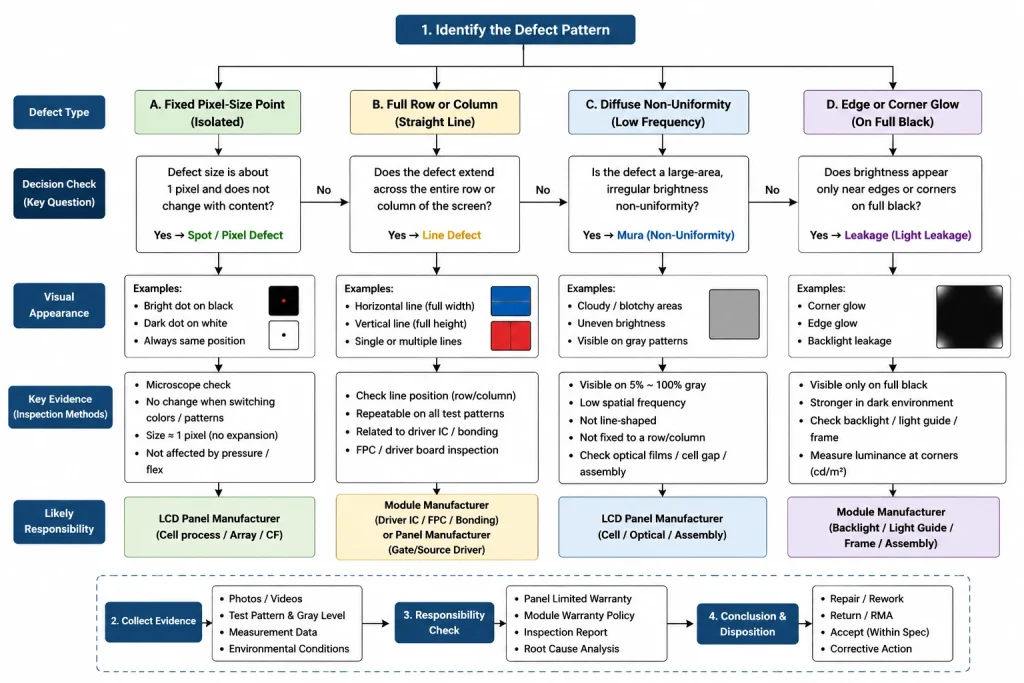
This guide separates four practical families: spot/pixel defects, line defects, mura or non-uniformity, and light leakage/backlight bleed. Black and bright spots are evaluated separately within the spot family because their visibility and contractual limits often differ.
Spot Defects — Black Spots and Bright Spots
Key distinction: A single dark subpixel (one of R/G/B) is typically an electrical defect in the TFT or data line driving that subpixel, and may be acceptable under industry standards like ISO 13406-2. A dark whole pixel (all three subpixels) is more likely caused by physical obstructions such as particle contamination or polarizer damage, and is generally considered a more serious defect regardless of zone. Always specify whether your acceptance criteria apply to subpixels or full pixels.
No universal grade table — Terms such as Grade A+, A, B, and C are supplier-specific unless the purchase agreement defines them. Store the numerical limits and visual samples, not only the grade name.
Industry reference: International standard ISO 13406-2 (and its successor ISO 9241-307) provides a framework for classifying pixel defects and defining acceptance criteria based on viewing distance and application type (e.g., Class I for professional use, Class II for general office, Class III for consumer, Class IV for non-critical). While these standards are not mandatory, referencing them in your incoming quality specification provides a neutral, vendor-independent baseline for negotiations.
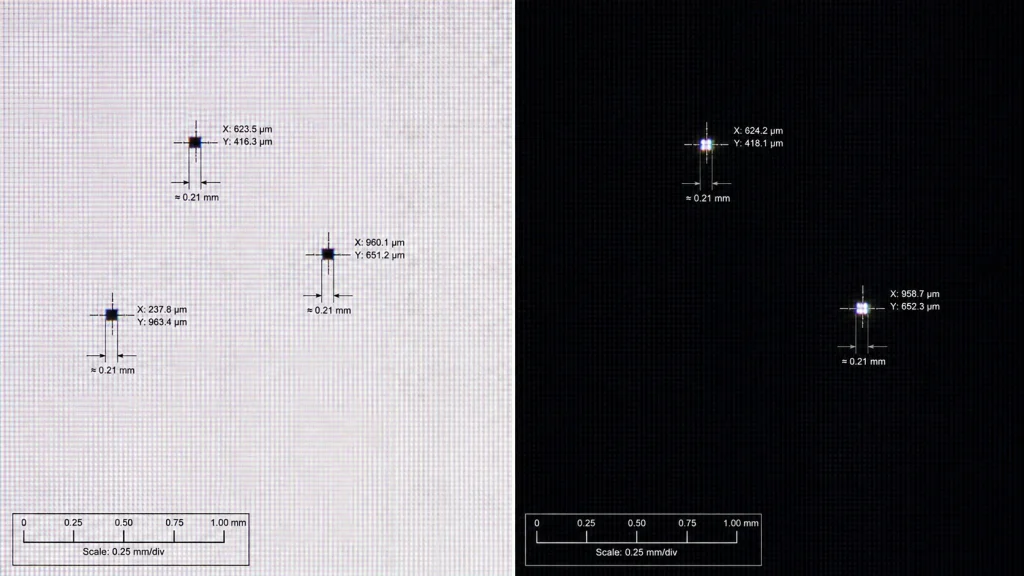
Spot defects are the most immediately visible LCD defect category during incoming quality inspection. They appear as single pixels or small pixel clusters that are permanently stuck in one state regardless of the image being displayed.
A black point can be an electrically dark pixel or subpixel, but larger dark spots may also arise from contamination, polarizer damage, pressure, or optical-stack defects. Classify pixel-level electrical defects separately from physical spots.
A bright point can result from a stuck subpixel or pixel, yet reflective contamination and local backlight defects can appear similar. Confirm the signature across black, white, red, green, and blue patterns before assigning cause.
Line Defects — Horizontal Lines and Vertical Lines
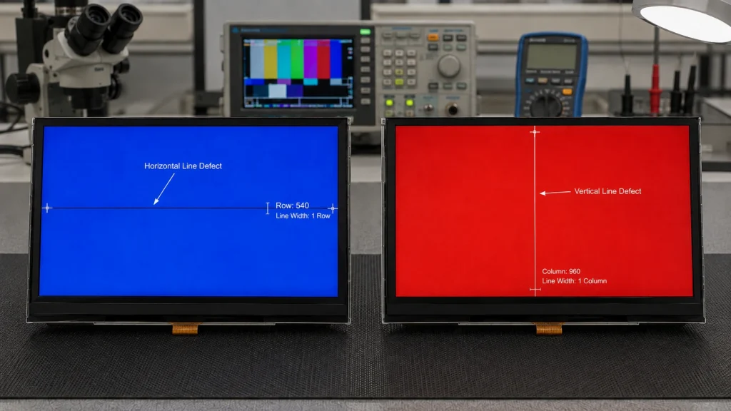
Line defects manifest as a continuous or segmented line running the full width (horizontal) or full height (vertical) of the display panel. Unlike spot defects which affect individual pixels, line defects indicate a failure in the panel’s driving circuitry.
A full horizontal line often points to a row/gate-drive path, while a full vertical line often points to a column/source-drive path. Partial lines can involve interconnects, COF bonding, cracks, driver channels, or signal/contact faults. Use electrical and mechanical diagnostics before assigning supplier responsibility.
Mura — Luminance and Color Non-Uniformity
Quick diagnostic checks: To distinguish between backlight-origin and cell-origin mura, change the brightness level. Backlight-origin mura (especially light guide patterns) scales with brightness, while cell-origin mura may appear or disappear at different gray levels. To distinguish between assembly-pressure and intrinsic mura, slightly loosen the mounting screws; if the pattern changes, it is likely due to mechanical stress rather than a panel defect.
Related Kadi Display reference: Kadi Display’s pressure-damage and mura analysis.
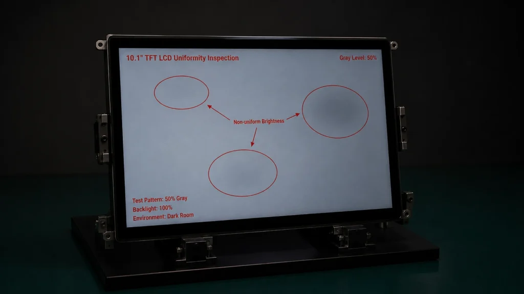
Mura is a Japanese term meaning unevenness or blemish, adopted by the display industry as the standard designation for non-uniform luminance or color across the panel surface. Unlike spot and line defects which are binary (present or absent), Mura is a gradient defect — it varies in severity and is subjective to evaluate.
Mura is not one mechanism. It can originate in cell-gap variation, rubbing/alignment, color filters, polarizers, compensation films, backlight/light-guide uniformity, driver voltage, optical bonding, or assembly pressure. Classification should describe the visible pattern first, then investigate root cause.
Mura evaluation must define gray levels, luminance, ambient light, viewing distance, angle, warm-up time, camera or observer method, and zoning. Without those conditions, two inspectors can reach different conclusions on the same panel.
Light Leakage — Backlight Bleeding and Structural Gaps
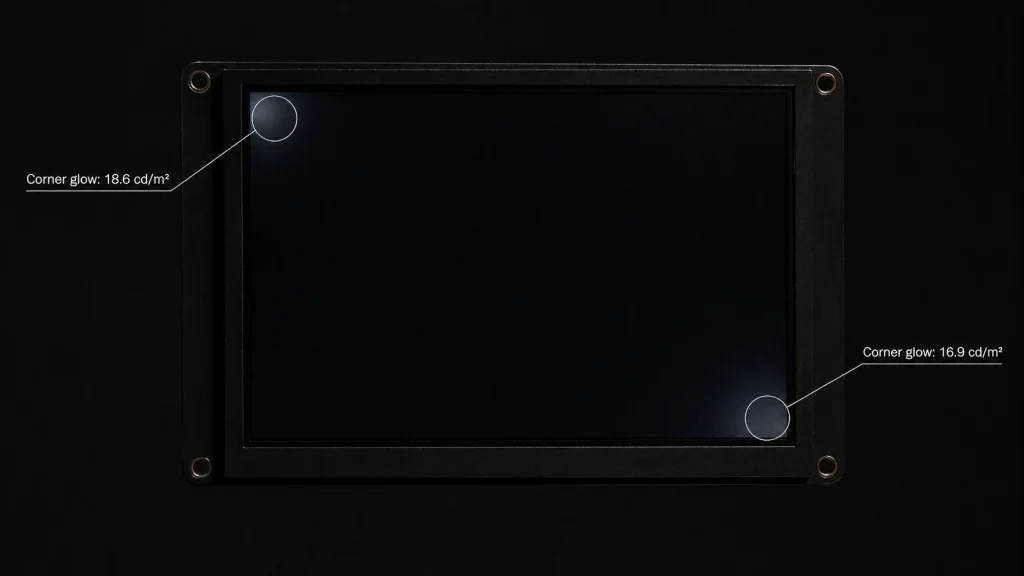
Light leakage refers to backlight illumination escaping the intended optical path and becoming visible to the user in areas that should display as black. It is most visible when displaying full-black content in a dark environment.
Two distinct physical mechanisms produce what is visually described as light leakage:
Backlight bleeding originates from within the LCD optical stack. The LED backlight enters the light guide plate at the edge and should distribute uniformly — but near the LED injection points, higher luminance is visible on full-black screens as bright glow areas, typically at corners or edges.
Structural light leakage originates from mechanical gaps in the display assembly. If the bezel frame does not seal completely against the LCD panel edges, backlight escapes around the perimeter.
Differentiating from LED aging: Uniformity issues that appear as patches of uneven brightness on black or gray screens can also result from LED driver current mismatch or LED aging. Unlike true light leakage (which is geometry-fixed and sharp-edged), LED-aging-related non-uniformity is typically diffuse, may appear gradually over time, and is usually more visible at higher brightness levels. If a panel passes incoming inspection but develops ‘leakage-like’ symptoms after months of operation, LED degradation may be the root cause. This distinction affects warranty responsibility: light leakage is a module-level defect, while LED aging may be considered wear-and-tear depending on the power-on hours and operating conditions.
Inspection Methodology — Equipment and Conditions
Acceptance evidence — A defensible defect decision contains the panel serial/lot, test pattern, brightness, warm-up, ambient light, distance, angle, zone, image or measurement, specification revision, and disposition.
Consistent defect identification requires standardized inspection conditions. The same panel can appear defect-free under bright ambient lighting but show obvious Mura and light leakage in a controlled dark environment.
Automated optical inspection can improve repeatability, but thresholds, lens shading, camera calibration, test patterns, and correlation with human-visible criteria must be controlled. AOI does not remove the need for a customer-approved visual standard.
Acceptance Criteria in Practice — Writing an Incoming Quality Specification
When symptoms change with handling, also review Kadi Display’s connector and interconnect failure guide.
The defect classification system above provides the vocabulary; translating it into a working incoming quality specification requires defining five parameters for each defect category:
- Detectable threshold: What size and contrast makes a defect countable? A spot defect visible only under 10x magnification is typically not counted. Standard practice: defects visible at 30 cm under standard ambient light are countable.
- Zoning: Is the panel divided into zones with different acceptance criteria? Many specifications use a central active area (inner 80%) with tighter limits and a peripheral zone with relaxed limits.
- Counting rules: How are adjacent defects counted? Two dark pixels separated by one functional pixel — is that one cluster defect or two spot defects? Standard: defects within 5mm are counted as one cluster.
- Cumulative limits: Does the total defect count across all categories have a combined maximum? Some specifications reject panels above a weighted total score across categories.
- Sampling plan: What percentage of incoming panels are inspected? AQL (Acceptable Quality Level) sampling per ISO 2859 is standard for batch inspection.
Responsibility should follow root-cause evidence. A line that changes when the connector is pressed may be a host-board or FPC contact problem rather than a panel-cell defect. A pressure mark aligned with a bezel boss may belong to the mechanical integration, even if the panel was clean at incoming inspection.
Use limit samples for defects that are difficult to express with one number. A photograph alone can be misleading because exposure and display settings change the appearance; preserve the original sample, viewing method, and instrument data where possible.
For safety-related interfaces, include UI zoning in the specification. A pixel defect inside an alarm icon or numeric field can receive a different disposition from the same defect in a decorative background area.
The inspection flow should separate detection from diagnosis. First record what the observer sees—position, size, color, shape, pattern dependence, angle dependence, and stability over time. Only then investigate likely mechanisms. Writing the suspected cause into the first inspection record can bias later analysis and supplier discussion.
Warm-up matters because backlight output, liquid-crystal response, and driver behavior can change after power-on. Define whether inspection occurs immediately or after a specified stabilization period. If the product uses automatic brightness or local compensation, lock those functions into a known state during comparison.
Camera-based measurement needs its own control plan. Fix exposure, focus, lens, distance, alignment, white balance, sensor linearity, and shading correction. A camera image intended only as a visual record should not be used to calculate luminance or chromaticity unless the system has been calibrated for that purpose.
Zoning should be tied to the user interface and active area. Document the zone boundaries in panel coordinates and explain whether borders, rounded corners, camera holes, or non-viewable areas are excluded. When the same display serves multiple products, the stricter UI layout may determine the shared incoming criterion.
A defect may change with mechanical state. Inspect the bare module, then repeat after integration if pressure, bonding, or bezel compression is a risk. Record screw torque, gasket compression, adhesive cure, and enclosure temperature. This step helps distinguish an incoming panel characteristic from damage introduced during assembly.
Line symptoms require connector checks before destructive analysis. Display a controlled pattern, inspect the FPC and ZIF lock, observe whether gentle pressure changes the line, and review timing or data errors. Avoid repeated flexing that could worsen an intermittent joint and destroy the original evidence.
Supplier communication improves when the record includes high-resolution images plus a schematic location and measurement. Mark the defect coordinates, active-area zone, pattern, brightness, viewing angle, and sample/lot. Ask for root-cause and containment evidence rather than accepting a replacement without learning whether the lot is affected.
Disposition should be explicit: accept, reject, use-as-is with documented deviation, rework, downgrade for a defined application, or hold pending analysis. Each exception needs authority, traceability, and expiration. Informal use of marginal panels can make field failures impossible to trace later.
Evidence Package and Release Control
Before releasing a industrial lcd defects design, convert the article’s guidance into a requirements matrix. Give every requirement an owner, source, revision, unit, tolerance, verification method, sample quantity, and acceptance rule. This prevents an informative article from being mistaken for a product specification and makes unanswered questions visible while changes are still inexpensive.
Separate documented limits from planning assumptions. A datasheet value, vendor application note, calculated estimate, measured prototype result, and internal design target do not have the same authority. Label each one. When a value is only representative, record the condition that would make it change and identify the exact document or test that must replace it before production release.
Use production-intent samples for the final decision. Evaluation boards, hand-selected cables, open-bench wiring, laboratory power supplies, and debug firmware can hide tolerance and assembly problems. Repeat the relevant checks with approved component alternatives, final connector and flex routing, enclosure constraints, released clock and power settings, and the intended manufacturing process.
Define failure evidence before testing. Decide which measurements, logs, images, waveforms, error counters, and sample identifiers will be collected when a unit fails. If the team records only pass/fail, intermittent or environment-dependent behavior becomes difficult to reproduce. Good failure evidence should distinguish component, interconnect, firmware, assembly, and system-level causes without immediately blaming the most visible part.
Control changes after approval. A supplier substitution, firmware update, timing adjustment, coating change, connector revision, PCB stack-up change, or new assembly site can invalidate earlier evidence. The change process should state which reviews and tests repeat, who approves deviations, how old and new lots remain traceable, and what field or incoming data will be monitored after release.
For publication, keep industrial LCD defects terminology consistent with the engineering record. Do not turn a conditional finding into a universal rule to make the prose sound decisive. Search engines and answer systems reward clear direct answers, but technical credibility depends on preserving scope, units, test conditions, and uncertainty. A qualified answer is more useful than a confident number that belongs to another component.
Complete the review with an independent reader. Ask someone who did not write the article or perform the first test to reproduce one calculation, locate each cited requirement, and challenge the main conclusion. Close any gap between the published guidance and the controlled engineering documents. This simple review often catches unit mistakes, stale revisions, hidden assumptions, and claims that cannot be verified from the evidence provided.
Archive the released package in a location shared by engineering, quality, procurement, and support. Include the article revision, approved drawings, links, calculations, test records, known limitations, and decision owner. That package gives later teams enough context to investigate a field issue or approve a controlled change without rebuilding the original reasoning.
FAQ: LCD Defect Inspection and Acceptance
Are black spots always dead pixels?
No. Pixel-level dark defects, particles, pressure damage, polarizer defects, and LC damage can all appear dark. Confirm size and behavior across test patterns and viewing angles.
Are line defects always a supplier rejection?
They are commonly serious, but disposition and responsibility depend on the contract and root cause. Connector, board, COF, panel, or mechanical stress can produce line-like symptoms.
What causes mura?
Mura is a visual class, not one cause. Cell, films, backlight, drive voltage, optical bonding, and mounting pressure are all possible contributors.
Can Grade A mean zero pixel defects?
Only if the supplier-customer specification defines it that way. Grade names are not interchangeable across vendors.
What makes an inspection repeatable?
Controlled patterns, brightness, warm-up, ambient light, viewing geometry, zoning, measurement method, limit samples, and a revision-controlled acceptance document.
Engineering source notes
Related Kadi Display reference: industrial LCD failure modes including mura and spot damage.
Related Kadi Display reference: pressure-induced LCD spots after installation.
Related Kadi Display reference: LCD connector failure modes and field diagnostics.
Primary technical references: Raspberry Pi display documentation; ASTM D3363 pencil-hardness method; MIPI D-PHY overview.
Product Reference & Engineering Support — For industrial TFT LCD modules, interface documentation, application review, sample validation, and OEM/ODM support, contact Sales@sz-kadi.com or review the Kadi Display product range.
Product range: industrial TFT LCD modules and custom display solutions.
Defect categories and methods are engineering guidance, not universal acceptance limits. Pixel counts, spot size, mura threshold, leakage limit, zone geometry, AQL, and disposition must be defined in the approved supplier-customer specification and validated for the intended use.
PREVIOR
MIPI DSI Bandwidth Guide: Lanes, Pixel Clock, and Data Rate per Lane
Siguiente
MIPI DSI and Capacitive Touch: Why the Interfaces Are Separate
Deja un comentario

Últimos blogs y noticias
- MIPI DSI Display Works at Room Temperature but Fails After Warm-Up: A Troubleshooting Workflow
- LCD Prototype Passed but Pilot Units Fail: A Display Integration Isolation Workflow
- LCD Controller Board Black Screen: A Safe Diagnostic Flow for EDID, Boot Order, Panel Timing, and Backlight
- VESA vs JEIDA LVDS Mapping: Evidence-Based Color Diagnosis and Release
- eDP LCD Panel Integration: Power, AUX, Link Training, Video and Backlight