
Casa
-
Blog & Notizie
-
Industrial Display Stack-Up Design: Integrating LCD, Touch, PCB, FPC, and Enclosure
Industrial Display Stack-Up Design: Integrating LCD, Touch, PCB, FPC, and Enclosure
2026-08-18
09:48
Industrial Display Stack-Up Design: Integrating LCD, Touch, PCB, FPC, and Enclosure
A practical engineering guide to mechanical fit, signal integrity, optical bonding, ESD/EMI, thermal control, and production release
A reliable industrial touchscreen is not created by choosing a good panel and then drawing a housing around it. It is created by controlling how every layer, cable, fastener, ground path, adhesive, and tolerance interacts from the cover glass to the main PCB.
What Industrial Display Stack-Up Design Actually Controls
When an HMI prototype shows edge light leakage, intermittent touch, a loose FPC, or pressure marks after assembly, the LCD is often blamed first. What actually happened is more mundane: the product team treated the display as one rectangular component instead of a controlled stack. Industrial display stack-up design defines the ordered layers, datums, clearances, compression zones, bend paths, grounding interfaces, and manufacturing tolerances that let the optical, electrical, and mechanical subsystems work together.
The problem-to-answer version is simple. If a display must survive temperature cycling, vibration, frequent touch, cleaning chemicals, and years of cable movement, the answer is not a stronger bezel alone. The answer is a stack whose loads bypass the active display area, whose flexible circuits are never used as structural members, and whose grounding and heat paths are intentional.
QUICK ANSWER: A production-ready stack-up identifies a common XY datum, a front-to-back Z budget, the active-area and component keep-outs, the permitted compression of seals and foam, the FPC service path, and the electrical reference between the display frame, PCB ground, and enclosure.
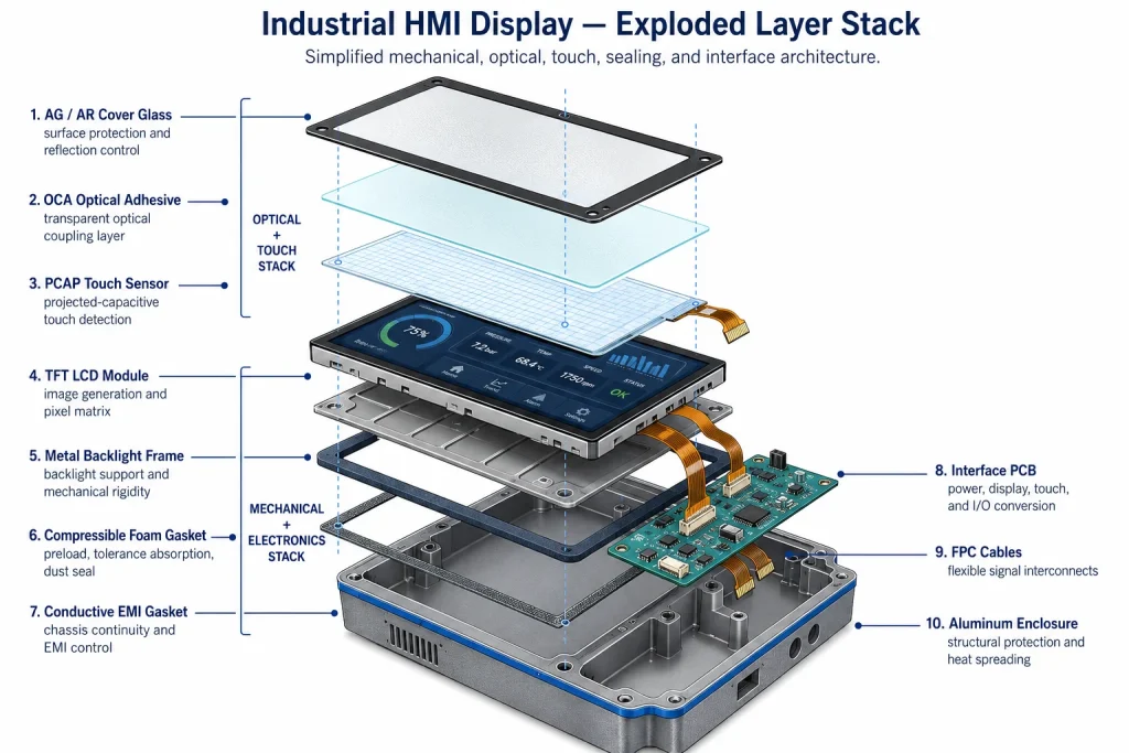
A typical stack includes cover glass, bonding layer or air gap, touch sensor, LCD, backlight frame, foam or gasket, bracket, FPCs, interface PCB, and enclosure. Every omitted drawing layer still exists in the physics.
Freeze Requirements Before the First Mechanical Layout
Stack-up work should begin while requirements are negotiable. Waiting until enclosure styling is fixed forces the display, connectors, heatsink, and service access into a volume that was never checked against supplier drawings.
Freeze four requirement groups. Optical requirements cover active area, viewing direction, brightness, reflections, black mask, and touch or lens construction. Environmental requirements cover temperature, impact, vibration, ingress, cleaning, UV, and condensation. Electrical requirements cover video and touch interfaces, backlight power, grounding, and cable reach. Manufacturing requirements cover assembly direction, rework, test access, and supplier tolerances.
Use the display drawing as a controlled interface
The released 2D drawing remains the contractual reference for outline, active area, component height, FPC position, bend restrictions, pinout, and tolerances. Carry one coordinate system through the LCD, cover glass, touch, PCB DXF, and enclosure CAD; different origins turn small translation errors into tooling changes.
- Define the viewing-area center and the LCD outline as separate controls; they are not always concentric.
- Record maximum component heights on both sides of the PCB, including connector locks and cable folds.
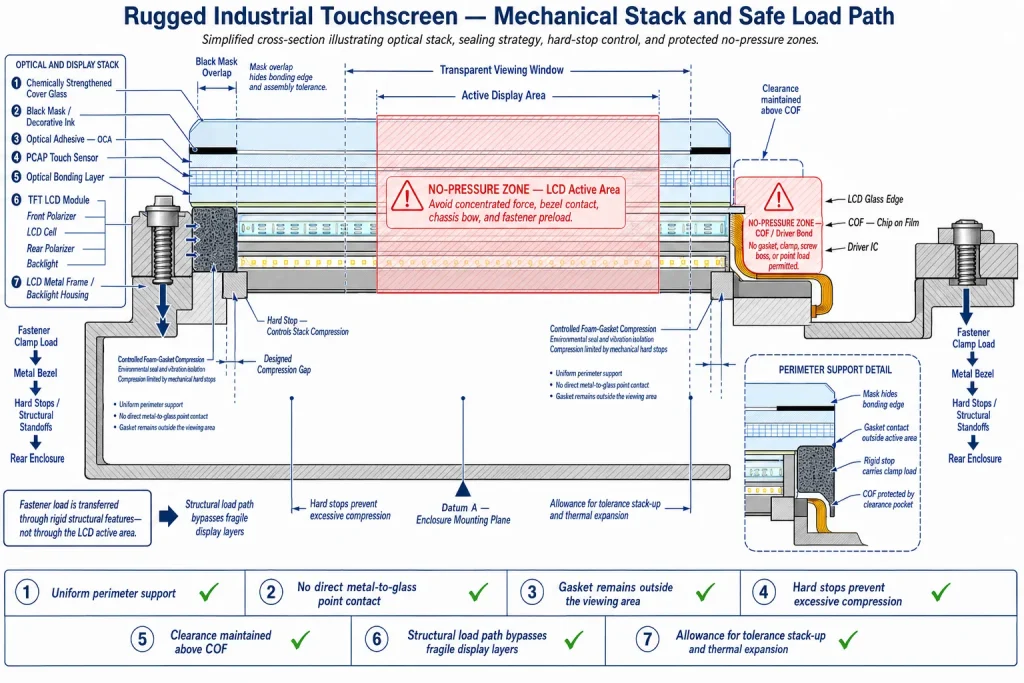
- Identify no-pressure zones over the active area, driver IC, chip-on-film region, and backlight light guide.
- Reserve assembly and tool access, not just final assembled volume.
- Track alternative panel sources only after comparing outline, active area, FPC exit, pinout, and optical stack.
DESIGN GATE: Do not approve the industrial design envelope until the preferred display and at least one realistic alternate have been overlaid in the same datum system. A nominally identical diagonal size or resolution does not guarantee mechanical interchangeability.
Build the Industrial Display Stack-Up from Front to Back
The front optical stack controls both what the user sees and how touch force reaches the enclosure. Cover glass thickness, black-mask overlap, surface coating, bonding method, adhesive modulus, touch-sensor construction, and bezel geometry should therefore be selected as one system.
Air bonding is economical and reworkable, but it introduces extra air interfaces and a cavity that must be managed against reflection, dust, and moisture. Optical bonding fills the gap with OCA or OCR, improving optical coupling and integrating the front structure. Select by environment and service strategy; Kadi Display’s air bonding versus optical bonding for industrial touchscreens comparison provides a useful decision framework.
Representative design ranges are starting points, not specifications. A cover lens may be roughly 1.1-3.0 mm thick, an OCA layer about 0.15-0.50 mm, and a structural foam gasket designed for about 20-40% working compression. The allowable values change with display size, glass treatment, foam grade, temperature, and impact requirement.
PRESSURE RISK: Never clamp the LCD active area or use the display frame to correct an enclosure flatness problem. Carry bezel and fastener loads into the metal frame or dedicated support lands, keep the chip-on-film region clear, and verify pressure mura at hot and cold limits.
PCB, FPC, Connectors, and Display Interface Integrity
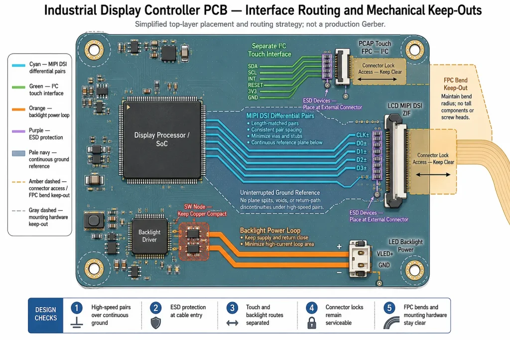
Mechanical packaging and signal integrity meet at the display connector. A connector can fit in CAD yet fail because its lock is inaccessible, the FPC folds against a stiffener edge, or high-speed pairs neck down near the board edge.
Place the connector so the FPC enters without twist, then model the cable in its assembled and service positions. Keep the first bend away from the stiffener transition. A practical initial rule is a bend radius of roughly 6-10 times the flex thickness for repeated motion, with supplier limits taking precedence. Provide strain relief that controls movement without crushing traces.
For MIPI DSI, route differential lanes as a transmission-line system. Protect pair geometry through the breakout, avoid reference-plane discontinuities, and keep backlight switching loops away from the lane bundle. The MIPI DSI PHY selection and PCB layout guide explains how interface choice, lane count, routing, and panel bring-up interact in industrial LCD systems.
MIPI ROUTING CHECK: A mechanical change that moves the connector can invalidate the electrical layout. Re-run impedance, length, return-path, ESD-placement, and cable-reach checks whenever the display or PCB origin changes.
Connector selection should reflect production volume. A 0.5 mm pitch ZIF is often more assembly-tolerant than a finer pitch, but pin count and board area govern the choice. Confirm contact orientation, pin 1, lock direction, insertion depth, and inspection access.
Mechanical Tolerances, Mounting, and Serviceability
Nominal CAD is not a tolerance analysis. The display, glass print, enclosure opening, gasket, bracket, screws, and adhesive all vary. At worst case, the stack must still avoid active-area clipping, hard-edge glass contact, and FPC interference.
Use a few functional datums: a primary plane for Z and flatness, plus orthogonal features for XY without over-constraint. Slots or compliant locators absorb thermal expansion. Hard stops limit gasket compression while foam or adhesive absorbs local variation.
Do not use screws to pull a warped enclosure flat across the display; the assembly may fail after plastic creep or thermal expansion. Specify bracket flatness, boss height, torque, and tightening sequence. For service replacement, provide a lift point and protect bonded cables.
Compatibility needs a drawing, not a label
A second-source LCD is compatible only when optical center, outline, thickness, FPC exit, connector, pinout, initialization, brightness, viewing direction, and environmental ratings fit the same system. Treat substitution as an engineering change.
Industrial Display Stack-Up Design for ESD, EMI, and Heat
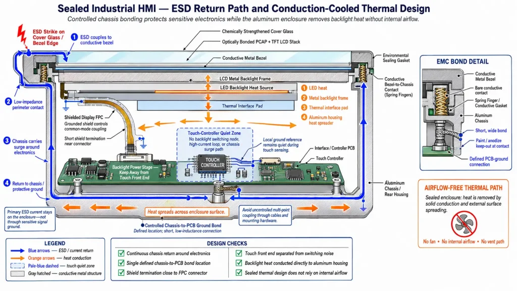
A display opening is both a user interface and an electromagnetic discontinuity. Glass can accumulate charge, the touch sensor is noise-sensitive, the LCD frame can float, and the interface cable can carry interference to the main board.
Create a deliberate chassis-ground strategy for the LCD frame, bezel, gasket, cable shield, and PCB. Define high-frequency return and ESD-diversion paths, then place protection near the entry so surge current avoids touch and display traces.
Thermal design is structural. High-brightness backlights and controllers can heat the center of a sealed assembly, changing adhesive stress, touch offset, liquid-crystal behavior, and plastic dimensions. Spread heat into the bracket or enclosure without creating a hard hot spot behind the LCD.
- Separate LED boost-current loops from touch-sensor and high-speed display routing.
- Use conductive gaskets only where compression, coating compatibility, and galvanic behavior are controlled.
- Keep ventilation or pressure-equalization features outside likely liquid and dust paths.
- Measure surface temperature and internal component temperature at maximum brightness, not only average UI load.
- Repeat touch and image checks during thermal soak; many faults disappear after the unit cools.
Verification Workflow and Common Failure Modes
The cheapest correction is a line moved before tooling. After bonding, enclosure tooling, and fixtures are released, even a 0.5 mm error can force changes to glass printing, adhesive die cuts, PCB placement, and firmware calibration.
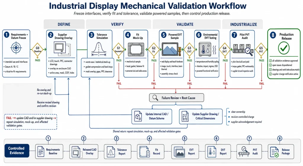
Use a staged verification plan that moves from geometry to function to environment. Each stage should have measurable acceptance criteria and an owner. A visual review alone cannot confirm connector retention, gasket compression, ESD current return, thermal stress, or assembly repeatability.
- Overlay released supplier drawings and run worst-case XY/Z tolerance analysis before detailed enclosure CAD.
- Build a non-functional fit sample to confirm optical center, bezel opening, FPC path, connector access, and assembly sequence.
- Test powered engineering samples for display timing, touch noise, backlight load, grounding, and cable sensitivity.
- Run thermal, vibration, impact, ESD, humidity, and cleaning exposure appropriate to the environment profile.
- Audit pilot production for torque, adhesive placement, gasket compression, cable insertion, inspection access, and rework damage.
From Stack-Up Review to Production Release
A good release package lets another engineer rebuild the intent. Archive the LCD and touch specifications, cover-glass drawing, bonding definition, stack-up cross-section, datums, PCB exchange, FPC bend drawing, connector specifications, grounding diagram, torque table, gasket die-cut, inspection criteria, and risk register.
The final review should ask one question repeatedly: what happens at worst case? Check maximum display thickness against minimum pocket depth, minimum bezel overlap against maximum active-area shift, maximum gasket compression against LCD pressure limits, and the shortest cable against the longest assembled route. Then repeat the same reasoning at hot, cold, wet, and aged conditions.
Frequently asked engineering questions
What is the most important datum in industrial display stack-up design? Use the display active-area center for optical alignment and a stable enclosure or bracket plane for Z control. Do not force one feature to control both functions if supplier tolerances make them independent.
Should the LCD frame be grounded? Often yes, but the connection method and ground domain must be intentional. Validate ESD and touch performance with the actual enclosure, coating, gasket, and cable shield.
Is optical bonding always better? No. It is valuable for bright, wet, dusty, high-vibration, or impact-prone environments, but air bonding may be preferred for lower-cost indoor products that require easier service. Evaluate the complete optical and mechanical stack.
Where should sourcing begin? Start with qualified industrial TFT LCD display modules, then freeze the mechanical, optical, interface, and environmental requirements that the complete assembly must meet.
Industrial display stack-up design succeeds when prototypes and production units assemble the same way and deliver the same image and touch behavior. Repeatability comes from shared datums, controlled loads, verified signal paths, realistic tolerances, and a complete release package.
PRODUCT REFERENCE & ENGINEERING SUPPORT: Explore Kadi Display’s industrial TFT LCD module portfolio o contact the engineering team for display selection, optical or air bonding, cover glass, touch integration, FPC customization, interface boards, and production-ready stack-up support.
Disclaimer: Dimensions and performance ranges in this guide are representative industry starting points, not universal design rules or compliance advice. Verify all limits against the selected LCD, touch panel, connector, adhesive, gasket, enclosure material, and applicable test standards. MIPI and other third-party trademarks belong to their respective owners.
PREVIDENTE
Existing Driver, Driver Modification, or New Driver? How to Check a Raspberry Pi CM4 MIPI DSI Panel Before Ordering
Prossimo
Optical Bonding vs Air Bonding for Industrial Touchscreens: Cost, Durability & Performance
Lascia un commento

Ultimi Blog & Notizie
- MIPI DSI Display Driver Development for Embedded Linux What Hardware Buyers Need to Confirm
- Why PCAP Touchscreens Need Retuning After Cover Glass Coating or Optical Bonding Changes
- Why Outdoor LCDs Fog Inside: Condensation, Sealing, Vents, and Heaters
- IP65 vs IP67 Industrial Displays: What the Rating Actually Covers
- How to Specify a Touchscreen for Food-Processing Equipment
Blog & Notizie correlate
-
 TN contro IPS2024-7-9
 -
TN contro IPS2024-7-9