GT911 I²C Address Problems: Why Your LVGL Touchscreen Is Not Detected
2026-06-30
17:48
GT911 I²C Address Problems:
Why Your LVGL Touchscreen Is Not Detected
The complete guide to GT911 addresses 0x5D and 0x14 — why the chip disappears from I²C scan results, how INT and RST pin states determine which address is active, pull-up resistor requirements, and every verified fix for the ‘GT911 not found at any known address’ error
By Kadi Display Technical Team | www.kadidisplay.com
The Most Frustrating Four Words in Embedded Touch Development
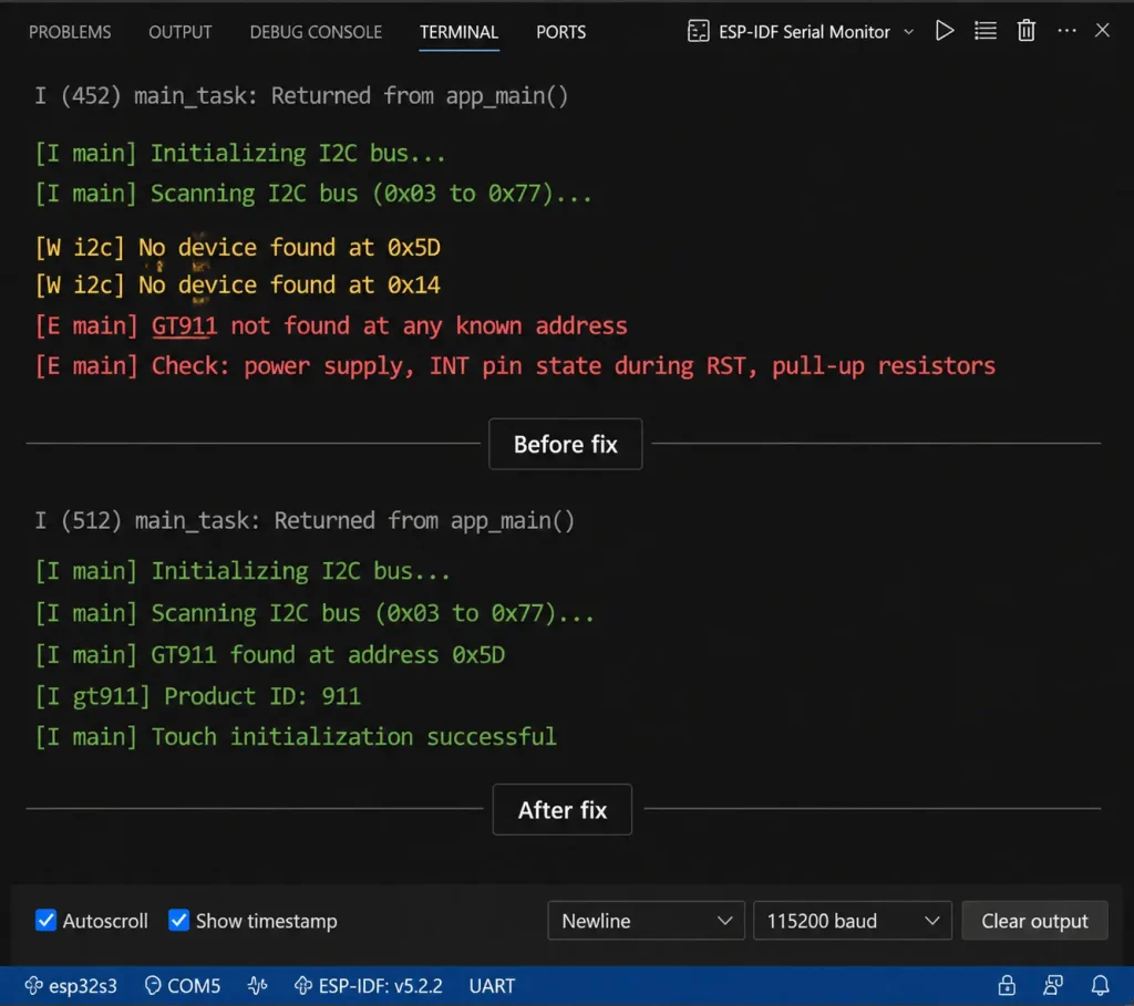
“GT911 not found at any known address.” This message — or some variation of it — appears in the logs of virtually every developer who integrates a GT911 capacitive touch panel for the first time. The display is on. The I²C bus is wired. The code is compiling. And the controller finds absolutely nothing.
The frustrating part isn’t the error itself. It’s that the GT911 is almost certainly physically functional. The chip is notoriously robust and rarely arrives dead from the factory. What’s happened, in the vast majority of cases, is one of a small set of hardware or firmware issues — specifically around how the GT911’s I²C address is assigned at startup — that makes the chip invisible to normal bus scanning without actually damaging it.
This article covers that mechanism in complete detail: how addresses 0x5D and 0x14 are determined, what the INT and RST pins actually do during power-up, what pull-up resistor values make or break I²C communication, and exactly how to diagnose which of the known failure modes is affecting your specific hardware. The guide is written around the ESP32-S3 and ESP-IDF v5.x environment — the most common platform for GT911-based industrial HMI and LVGL kiosk display development — but the hardware diagnostics apply universally.
·
How GT911 I²C Address Assignment Actually Works
The GT911 does not have a resistor-selectable address like many I²C sensors. It does not use solder bridges. It does not read a configuration pin at a stable logic level. The address is determined by a one-time sampling event that happens during the power-on reset sequence — specifically, at the precise moment the RST (reset) pin transitions from LOW to HIGH. Whatever voltage level the INT pin is at during that transition determines the I²C address for the entire power cycle.
INT pin LOW when RST releases → I²C address 0x5D. INT pin HIGH when RST releases → I²C address 0x14. That’s it. The address is latched internally and does not change until the next power cycle or hardware reset. There is no way to read or change the address after it’s been set without cycling the RST pin.
This mechanism is well-documented in the GT911 programming guide but is routinely misunderstood because it differs from every other I²C device most embedded engineers have worked with. The consequence of misunderstanding it: a firmware that assumes 0x5D but inadvertently holds INT HIGH during reset initialization will find the GT911 at 0x14 — and a scan that only checks 0x5D will conclude ‘no device found’ even when the hardware is completely functional.
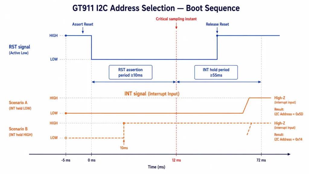
The Timing Window That Determines Everything
The INT pin must be held at the target level for a specific period after RST releases. The GT911 specification requires INT to be held for at least 55 ms after the RST rising edge before it’s released to floating/interrupt-input mode. During this window, INT must be actively driven — not just pulled — to ensure the level doesn’t drift due to parasitic capacitance or a weak pull resistor during the sampling period.
The complete validated reset sequence for address 0x5D:
To select address 0x14 instead, set INT HIGH in Step 1 (gpio_set_level(INT_PIN, 1)) and keep all timing the same. Everything else in the sequence is identical.
Why Most Tutorials Get This Wrong
Many LVGL and ESP32 tutorials initialize the GT911 with a simplified reset sequence: RST LOW briefly, RST HIGH, then immediately configure INT as an interrupt input. This works inconsistently. At room temperature on a clean bench with no other I²C devices, INT may happen to be LOW when RST releases, causing the chip to appear at 0x5D. But on a different board revision, temperature, or PCB layout, INT may float high during the 55 ms window, and the chip silently moves to 0x14.
This explains why the ‘GT911 not found’ error appears intermittently on some boards but consistently on others — it is directly correlated with the INT pin’s actual voltage during the reset window. The fix is always the same: explicitly drive INT to the desired level for the full 55 ms window before releasing it.
📌 Quick Mental Model
Think of the GT911’s I2C address selection as a combination lock that’s only accessible during a narrow window. The ‘combination’ (INT level) must be set before the lock closes (RST releases). Once RST goes HIGH, the address is fixed until the next power cycle. Nothing in firmware can change it afterward — only a RST pulse can reopen the window.
Pull-Up Resistors — The Silent Cause of ‘Not Found’
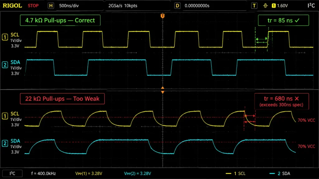
After incorrect reset sequencing, missing or wrong pull-up resistors are the second most common cause of GT911 not being detected. I²C is an open-drain protocol — the bus lines are only ever actively pulled LOW, never actively driven HIGH. The pull-up resistors are what bring SDA and SCL back to the logic-HIGH state. Without them, or with resistors that are too weak or too strong for the bus speed, communication either never starts or fails partway through every transaction.
The Physics of Pull-Up Resistor Sizing
The I²C specification defines maximum rise time requirements that determine the minimum pull-up strength. At 400 kHz, the maximum allowed rise time from GND to 70% of VCC is 300 ns. Rise time is determined by: t_rise = 0.8473 × R × C_bus, where R is the pull-up resistance and C_bus is the total bus capacitance.
With typical bus capacitance of 50–100 pF, the maximum pull-up resistance at 400 kHz is approximately:
R_max = 300 ns / (0.8473 × 100 pF) ≈ 3.5 kΩ
In practice, 4.7 kΩ pull-ups work reliably with bus capacitance below 50 pF. If the FPC cable from host to display module is longer than 100 mm, adding cable capacitance may push you below the rise time margin. In that case, drop to 2.2 kΩ pull-ups. Pull-ups below ~1 kΩ draw excessive quiescent current and can interfere with I²C low-level detection if the transmitter’s current sink is insufficient.
Diagnosing Pull-Up Problems Without an Oscilloscope
If you don’t have an oscilloscope available, a multimeter in DC voltage mode can reveal the most critical pull-up failure. With the I²C bus idle and power applied:
- SDA and SCL must both read VDDIO. If either reads 0 V, the line is stuck LOW — either the GT911 is actively pulling it down, a pull-up resistor is missing, or a pull-up resistor is connected to the wrong supply rail.
- If SDA reads ~0.7 V or ~1.2 V at idle, there is a voltage divider effect from a pull-up to the wrong rail meeting another device’s input clamping.
- If both read VDDIO but I²C scan still fails, the issue is timing-related rather than missing pull-up. Reduce resistance or reduce bus speed to 100 kHz.
Systematic Diagnosis — Eight Reasons GT911 Is Not Found
When an I²C scan returns nothing at 0x5D or 0x14, one of the following eight causes is responsible. They are listed in order of frequency — the first two account for approximately 70% of all GT911 ‘not found’ reports in developer community threads.
R1 INT Pin Floating or Wrong Level During Reset
Symptom: Scan finds nothing at 0x5D; device may be at 0x14 or vice versa. Behavior inconsistent between power cycles.
Root Cause: INT pin not actively driven during reset sequence. GT911 latches whichever address corresponds to the floating level.
Fix: Explicitly drive INT as GPIO OUTPUT to 0 for 0x5D or 1 for 0x14 during the reset sequence. Hold for 60 ms after RST releases before switching INT to GPIO INPUT.
R2 Missing Pull-Up Resistors on SDA or SCL
Symptom: I²C scan finds nothing at any address. SDA or SCL reads near 0 V at idle. Firmware may report I2C bus error or timeout.
Root Cause: Open-drain I²C lines have no path to logic HIGH without pull-ups. Every transaction fails immediately.
Fix: Install 4.7 kΩ resistors from SDA and SCL to VDDIO. Verify both lines read VDDIO at idle with a multimeter before powering up.
R3 RST Pulse Too Short — GT911 Never Fully Initializes
Symptom: Device found at correct address. I²C ACKs are received. But all register reads return 0x00 and no touch events are generated.
Root Cause: RST LOW pulse shorter than the minimum 10 ms. Internal state machine does not complete power-on sequence.
Fix: Ensure RST is held LOW for ≥12 ms using a calibrated delay. Verify with a logic analyzer if needed.
R4 VDDIO Level Mismatch — GPIO at Wrong Voltage
Symptom: GT911 not found in scan. No response at either address. SDA and SCL may read VDDIO correctly but no ACK is returned.
Root Cause: Host MCU GPIO operates at 3.3 V but GT911 VDDIO is 1.8 V. The GT911 sees RST and INT as permanently HIGH, causing incorrect address selection and possible damage risk.
Fix: Check VDDIO voltage at GT911 pin. If VDDIO = 1.8 V, use a 1.8 V GPIO bank or a bidirectional level shifter.
R5 Another Device Occupying 0x5D or 0x14
Symptom: I²C scan finds a device at 0x5D or 0x14 but GT911 touch reads are wrong or garbled.
Root Cause: Another I²C device on the same bus shares the GT911 address. Both devices ACK the same address, causing read corruption.
Fix: Run a full I²C scan from 0x03 to 0x77. If conflict exists, switch GT911 to the other address by holding INT HIGH during reset.
R6 Wrong I²C Port or GPIO Pins in Firmware Configuration
Symptom: Scan finds nothing. Hardware appears wired correctly. Probing SDA/SCL shows expected pull-up levels.
Root Cause: Firmware configures I²C peripheral on different GPIO pins than where the module is physically connected.
Fix: Cross-check firmware GPIO numbers against PCB schematic one by one. Probe the configured pins with a scope.
R7 FPC Cable Not Seated — Open Circuit on SDA or SCL
Symptom: GT911 not found. SDA and SCL read VDDIO, but no device responds. Signal exists on host side but not at display module end.
Root Cause: ZIF FPC connector is not fully latched, or SDA/SCL trace is physically open.
Fix: Measure continuity between host PCB SDA/SCL and the FPC connector pads at the module end. Reseat the FPC cable and relatch the ZIF connector.
R8 ESP-IDF I²C Driver Not Installed Before Scan
Symptom: Firmware compiles and runs, but scan returns no devices. Identical hardware works with a different code example.
Root Cause: I²C driver is configured with i2c_param_config() but i2c_driver_install() is not called, or is called with incorrect parameters.
Fix: Verify both functions are called and return ESP_OK. Check the I²C port number is consistent across all read/write calls.
The Four-Step Verification Protocol
Once you’ve addressed the likely cause based on the diagnosis above, verify the fix in a specific sequence. Each step must pass before proceeding to the next — don’t skip ahead, because later steps depend on earlier ones being correct.
Step 3 — reading the product ID — is the most reliable single indicator of a correctly initialized GT911. Here’s the complete code:
Address Configuration in ESP-IDF / LVGL Stack
Once you’ve confirmed the GT911 is alive at the correct address, the address must be correctly propagated through the driver stack. There are three places in the ESP-IDF / LVGL integration where an address mismatch causes ‘not detected’ or silent failure:
esp_lcd_panel_io_i2c_config_t — Primary Address Setting
Confirming the Correct Address Constant Values
In the esp_lcd_touch_gt911 component, the address constants are defined as:
⚠ Common Address Confusion
Community forums frequently suggest ‘just try both addresses.’ This works for getting the driver running but leaves the underlying reset sequence bug unfixed. On the next power cycle, if something changes INT pin behavior, the GT911 may switch addresses again. Fix the reset sequence, then configure the address to match.
Hardware Design Recommendations for Reliable Address Selection
If you’re at the PCB design stage rather than bring-up debugging, these design practices eliminate the GT911 address selection problem before it reaches prototyping.
Getting a Module That Works Out of the Box
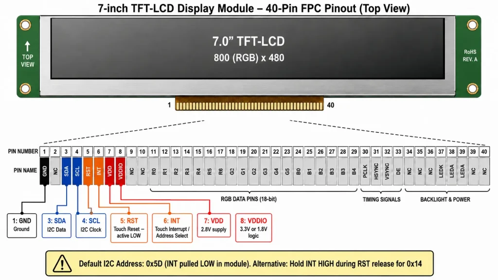
A significant portion of GT911 ‘not found’ reports originate not from firmware bugs or PCB design errors, but from display modules where the GT911’s factory configuration doesn’t match the default assumption — or where the module’s FPC pinout places the INT and RST lines at unexpected positions that conflict with the recommended reset sequence.
When evaluating GT911-equipped display modules for industrial HMI or embedded kiosk applications, there are four documentation deliverables that reliably distinguish a supplier who supports embedded integration from one who doesn’t:
- GT911 factory configuration binary (186-byte config block) — confirms the active area dimensions are correctly set for the panel size and provides the baseline sensitivity parameters.
- FPC connector pinout with INT and RST positions identified — enables correct firmware configuration without reverse-engineering from hardware probing.
- Confirmed I²C address at factory (0x5D or 0x14) — tells you whether INT is pulled low or high in the module’s default state, which determines whether you need to match it or override it.
- VDDIO voltage specification — determines whether level shifting is required between the module and the host MCU’s GPIO bank.
Kadi Display’s industrial TFT touch display modules provide these four items as standard deliverables, with factory-calibrated GT911 configuration, confirmed default I²C address, and full FPC pinout documentation. For teams selecting display technology for a broader embedded HMI project, their TFT LCD display essential guide for industrial and medical use covers display interface selection, panel technology trade-offs, and integration considerations across the full spectrum of industrial display applications.
Summary — What to Check Before Opening Another Forum Thread
The ‘GT911 not found at any known address’ error is almost always caused by one of a small set of deterministic hardware and firmware conditions. Before searching community forums, work through this list in order:
Product Reference & Engineering Support
For GT911-equipped industrial TFT-LCD touch display modules with factory-confirmed I²C address, full FPC pinout documentation, and GT911 configuration binary, contact Kadi Display at Sales@sz-kadi.com. Browse industrial TFT touch display modules →
Disclaimer: Code examples, schematic details, and timing values in this guide are provided for educational reference and must be validated against your specific hardware. GT911 behavior may vary between firmware revisions; always consult the official Goodix GT911 programming guide for authoritative specifications. GT911 is a trademark of Shenzhen Goodix Technology Co., Ltd. ESP32-S3 is a trademark of Espressif Systems. LVGL is open-source software under MIT license. All other trademarks are the property of their respective owners. No affiliation with any third party is implied.
Leave A Comment

Latest Blog & News
- GT911 I²C Address Problems: Why Your LVGL Touchscreen Is Not Detected
- GT911 Touchscreen Not Working with LVGL? A Hardware and Software Checklist
- How LED Backlight Lifetime Affects Industrial TFT LCD Display Reliability
- Air Bonding vs Optical Bonding: How to Choose for Industrial Touchscreens
- What Is a Wide Temperature LCD Display and When Do Industrial Devices Need One?