
Главная
-
Блог & Новости
-
Display Bridge IC Selection: Direction, Bandwidth, Features and Productization
Display Bridge IC Selection: Direction, Bandwidth, Features and Productization
2026-09-24
10:08
Display Bridge IC Selection: Direction, Bandwidth, Features and Productization
FIRST GATE RST GATE Direction and protocol roles
SIZING BASIS NG BASIS Complete timing, format and link limits
Draw the Directional Signal Chain
STOP / SAFETY GATE ETY GATE Write the conversion direction and source/sink roles before naming a device. Y-to-X support is not evidence for X-to-Y; a familiar connector or resolution does not prove direction, clocking or initialization.
Draw the Directional Signal Chain First
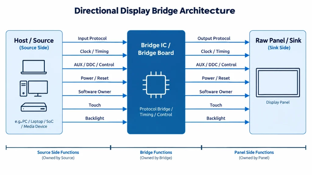
Interface labels do not describe endpoint roles. HDMI, DisplayPort/eDP, MIPI DSI, LVDS/OLDI, RGB, and USB-C display paths each have source/sink or host/device behavior, control channels, link setup, and electrical requirements. Write the entire path with arrows and exact endpoints before searching for a device.
For example, “DSI to LVDS” means the processor is a DSI host, the bridge receives DSI, the bridge transmits LVDS/OLDI, and the panel receives that stream. Reversing the endpoints is a different design. Likewise, “HDMI and LVDS” on a distributor page does not establish whether a part accepts HDMI and outputs LVDS, performs the reverse conversion, or belongs to a board containing additional processing.
KadiDisplay’s industrial display interface guide gives the wider system context. If the source is a standard external video port rather than a native embedded pixel pipeline, the custom TFT-to-ProAV/controller guide helps decide whether the system needs a bridge, a scaler/controller, or a complete display input stage.
Freeze Both Endpoint Contracts
Both sides of the bridge need exact roles, versions, timing, format, lanes, voltage domains and software ownership before a device can be shortlisted.
Create two endpoint records. The source record should include processor and display engine, protocol/role, supported lane or channel count, per-lane rate or clock range, pixel clock and active timing, blanking, sync polarity/format, pixel format, color depth, clock topology, control bus, software stack, power domain, and boot behavior. The sink record should capture the panel’s exact part and revision, input protocol, lanes/channels/ports, link or clock range, native timing and tolerances, mapping, voltage and common-mode requirements, power sequence, backlight boundary, connector and pinout.
Do not copy only the resolution. A 1920 × 1080 image can be transported with different blanking, refresh, color format, depth, lane allocation, mapping, or link rate. Some bridges constrain horizontal or vertical values, reference-clock ratios, burst/non-burst behavior, synchronization mode, or combinations of lanes and clocks. Datasheet maxima should not be combined independently into a configuration the device never promises to support.
Calculate With Complete Timing and Explicit Overhead
Bandwidth feasibility must start from complete timing and device-specific packing rather than active resolution alone.
Calculate Timing and Bandwidth With Real Blanking
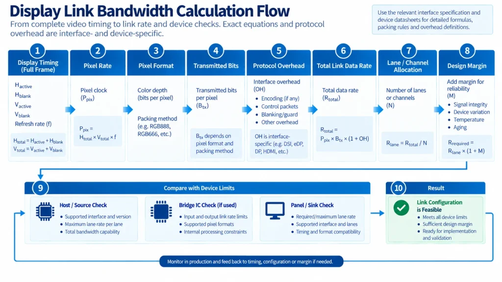
Begin with the complete timing, not active pixels alone. Pixel clock is based on horizontal total × vertical total × refresh rate for a conventional raster timing. Transport capacity then depends on color depth, pixel encoding, protocol overhead, lane/channel count, and device architecture. Use the protocol and device documentation rather than applying one generic efficiency factor across HDMI, DisplayPort/eDP, DSI, and LVDS/OLDI.
A bridge has two independent capacity questions: can its input receive the source stream, and can its output generate the panel stream? Internal clocking, FIFOs, PLL ranges, and timing constraints connect those sides. A design can fit a headline “maximum resolution” yet fail because the exact pixel clock, blanking, lane arrangement, color depth, or output clock falls outside an allowed combination.
Record normal, tolerance, and corner values. Include spread-spectrum behavior if used, reduced-blanking assumptions, refresh variations, and boot or fallback modes. Treat any configuration obtained only from a forum or evaluation-board default as an experiment until it is supported by the device and endpoint evidence.
Identify Functions the Bridge Does Not Supply
A plausible protocol pair can still fail when scaling, color, descriptors, protection, panel services or software support is missing.
Check the Features That Commonly Break an Otherwise Plausible Match
Scaling and frame-rate conversion
Most simple bridges are not universal scalers. If source timing must become a different active resolution, aspect ratio, refresh, or scan format, select a device explicitly designed for that processing or change the source timing. A small FIFO used for clock-domain handling does not establish arbitrary frame buffering or scaling.
Color, depth, and LVDS/OLDI mapping
Confirm RGB versus YCbCr behavior, 18/24/30-bit support as applicable, dithering, channel order, sync/data-enable handling, and limited/full-range assumptions. For LVDS/OLDI outputs, verify single/dual-link or port configuration, odd/even pixel allocation, channel order, and VESA/JEIDA-style bit mapping. TI’s HDMI/DVI-to-LVDS application report is a useful conceptual reference, but the exact bridge and panel documents govern the implementation.
EDID, DPCD, HPD, AUX, DDC, and control roles
An external video source may expect EDID over DDC and hot-plug behavior. An eDP/DisplayPort path uses AUX transactions, DPCD capabilities, link training, and HPD behavior according to the implementation. A raw fixed-timing panel may expose no EDID. Determine whether the bridge passes, stores, synthesizes, or ignores these functions and who owns the data.
Backlight, touch, audio, and HDCP
A display bridge does not automatically solve the backlight driver, touch interface, audio, content protection, or power-supply design. Some parts offer PWM/GPIO or selected auxiliary functions; treat these as explicit features with electrical limits and software ownership. If protected content is in scope, review licensing, key provisioning, supported versions, repeater behavior, and production security with the device supplier and legal/compliance owners.
Use Device Examples to Understand Boundaries, Not to Skip Selection
Texas Instruments describes the SN65DSI83 as a MIPI DSI-to-single-link LVDS bridge and the SN65DSI86 as a MIPI DSI-to-embedded DisplayPort bridge. These examples show why direction and output family matter: devices that share “DSI bridge” language do not target the same panel interface. Their exact lane counts, rates, resolutions, packages, temperature grades, clocks, features, and software requirements must be checked in current product documentation.
Do not select a production component merely because an evaluation board displayed an image. Record the board schematic revision, device marking, strap states, register dump, firmware/software, source timing, panel timing, cables, power supplies, and any undocumented patches. Then reproduce the function on the intended architecture.
Часто задаваемые вопросы
Use these answers to reject three shortcuts before investing in a schematic or custom PCB.
Is an HDMI-to-LVDS bridge the same as an HDMI LCD controller board?
Not necessarily. A controller board commonly includes input handling, EDID, scaling, OSD, panel timing, backlight and power functions. A bridge may only translate the protocol/format under constrained timings. Inspect the complete architecture.
Can a bridge IC change resolution or refresh rate?
Only if its documentation explicitly provides the required scaler or frame-rate behavior. Many bridges expect compatible input and output raster timing.
Is a Linux driver enough to prove hardware compatibility?
No. It can reduce software risk, but the exact chip revision, board wiring, clocks, power, device-tree/configuration, source mode and panel still require engineering validation.
Cross the Evaluation-Board Gap Before Release
The final decision includes power, clocks, reset, layout, drivers, recovery and production evidence—not only an evaluation-board demo.
Design Power, Clocks, Reset, and Software as One Subsystem
A bridge often needs multiple rails, I/O-domain compatibility, a reference clock or recoverable input clock, reset timing, strap sampling, and control-bus access. The panel has its own rail and backlight sequence. Build one timing diagram covering source, bridge and panel; identify which device can drive each signal before the next domain is alive.
Software ownership must be explicit. Decide whether configuration resides in boot firmware, kernel driver, device tree, microcontroller, EEPROM, strap pins, or bridge nonvolatile memory. Linux systems may use the DRM bridge framework to represent chained encoders/bridges, but availability of a framework does not prove that the exact device, mode, board wiring, and panel are supported. Confirm driver status, upstream versus vendor code, required patches, configuration bindings, error reporting, resume behavior, and long-term maintenance.
Close the Evaluation-Board-to-Product Gap
Evaluation modules hide risk by supplying known-good power, oscillators, level shifting, impedance control, connectors, protection, firmware, and sometimes additional devices. Before committing to a custom PCB, compare the evaluation design with the intended product line by line.
- Confirm every power rail, ramp, decoupling network, reset source, strap and reference clock.
- Recalculate high-speed routing for the chosen stack-up, connector, cable, vias, reference planes and return paths.
- Verify I/O voltage compatibility, pull-ups, open-drain behavior and power-off leakage.
- Decide whether ESD protection, common-mode chokes, AC coupling or level translation is permitted by each link.
- Capture thermal loss and junction-temperature margin at worst-case mode and environment.
- Lock the software/register configuration and preserve a diagnostic register dump.
- Confirm component lifecycle, orderable suffix, package assembly, regulatory/material declarations and alternate strategy.
В tools and accessories category may help with development boards or cabling, while the FPC and connector design guide covers the interconnect boundary. Availability and exact compatibility must be confirmed for the named source, bridge, panel and board revision.
Validate the Whole Path and Preserve the Evidence
Bring up the lowest-risk supported mode first. Capture source mode, bridge status and register state, measured clocks/rails, panel output timing, link error evidence where available, and a known test pattern. Then expand to every required mode and corner.
Create a Bridge Selection Evidence Sheet
Use one status-driven evidence sheet at schematic review instead of repeating the full endpoint and validation checklists. The sheet should expose what is proven, what remains conditional, who owns closure, and which artifact supports the decision.
Use green only for a cited or measured result. A yellow item needs an owner, next evidence, and closure date; red stops release. When the source, bridge silicon, panel, firmware, cable, or mode set changes, reopen the affected rows and document why the remaining evidence still applies. Include negative tests for unsupported modes, absent-panel behavior, invalid configuration, missing clock or failed control response when those cases are safe and relevant.
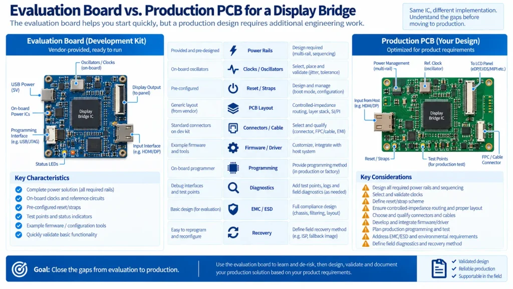
RELEASE GATE ASE GATE Release the bridge path only when one named source-to-panel configuration has a supported operating point, controlled power and software ownership, measured final-board evidence, diagnosable failure behavior, and a reproducible manufacturing/service record. A working evaluation-board image is an intermediate milestone, not the release decision.
KadiDisplay can review the proposed path through the engineering contact page; provide the directional chain, exact source and panel, complete timings, bridge suffix, power/clock plan, firmware owner, PCB/cable constraints, operating environment, and unresolved evidence gaps.
Primary Sources
- Texas Instruments display-interface bridge selection guide
- Texas Instruments SN65DSI83 product page
- Texas Instruments SN65DSI86 product page
- Linux DRM/KMS helpers documentation
ENGINEERING DISCLAIMER SCLAIMER This selection method does not approve a bridge IC, register script, evaluation-board schematic, or PCB layout. Device limits are conditional: do not combine independent headline maxima into an operating point the exact silicon revision does not support. Verify direction, endpoint roles, timing totals, packing, clocks, rails, I/O domains, reset and strap behavior, mapping, software ownership, errata, and layout against current device and endpoint documentation. Use licensed standards where required and validate the final PCB, connector, cable, panel, firmware, environmental state, and protected-content path before release.
Предыдущий
LCD Prototype Passed but Pilot Units Fail: A Display Integration Isolation Workflow
Следующая
LCD Controller Board Black Screen: A Safe Diagnostic Flow for EDID, Boot Order, Panel Timing, and Backlight
Оставить комментарий

Последние блоги и новости
- USB Touchscreen Keeps Disconnecting in an Industrial HMI: A Fault-Isolation Workflow
- HDMI Monitor Works on a Laptop but Not an SBC: EDID, HPD, and Timing Checks
- MIPI DSI Display Works at Room Temperature but Fails After Warm-Up: A Troubleshooting Workflow
- LCD Prototype Passed but Pilot Units Fail: A Display Integration Isolation Workflow
- Display Bridge IC Selection: Direction, Bandwidth, Features and Productization
Блог и новости
-
 TN против IPS2024-7-9
 -
TN против IPS2024-7-9