
MIPI, LVDS, RGB, and Touch FPC Connector Design Guide
2026-08-05
11:58
MIPI, LVDS, RGB, and Touch FPC Connector Design Guide
How interface speed, return paths, connector geometry, FPC construction, and mechanical retention change the design
An FPC connector must be chosen for the complete electrical and mechanical channel—not from pitch and pin count alone. This guide explains what changes between RGB, flat-panel LVDS, MIPI DSI, and capacitive-touch interconnects and shows which claims require simulation, measurement, or exact component data.
Why Each Display Interface Demands a Different Connector Approach
Direct answer — Pitch and pin count establish mechanical compatibility. Interface-specific channel data, pin assignment, return paths, current rating, FPC stack-up, and retention establish whether the connection will work reliably.
Related Kadi Display reference: Kadi Display’s MIPI, RGB, and LVDS interface selection guide.
Industrial display engineers sometimes select the FPC connector from pitch, circuit count, and lock style, then review signal integrity later. That sequence is risky for every interface with fast edges. RGB may operate at a lower fundamental clock than serialized links, but rise time, trace length, return path, and simultaneous switching can still make the connector electrically important.
The same connector family can serve different interfaces, but the channel requirements change: single-ended versus differential signaling, edge rate, return-current geometry, insertion loss, crosstalk, current delivery, ESD exposure, and cable support. The connector footprint and FPC termination are part of that channel.
This guide examines each major industrial display interface from the connector perspective specifically — what the connector must do differently for RGB, LVDS, MIPI DSI, and capacitive touch.
RGB Parallel Interface Connectors — High Pin Count, Low Signal Integrity Risk
The RGB parallel LCD interface transmits pixel data as single-ended signals across 16 to 24 data lines plus timing signals (HSYNC, VSYNC, DE, PCLK). This results in connectors with 40 to 54 pins — the highest pin count of any standard display interface.
RGB is often more tolerant than multi-gigabit serial links, yet it is not automatically low-risk. Verify PCLK and data-edge quality, ground distribution, simultaneous switching, cable length, voltage, and timing at the receiver. A wide, high-pin-count flex also needs even insertion and retention across its contact field.
LVDS Interface Connectors — Differential Pairs Change Everything
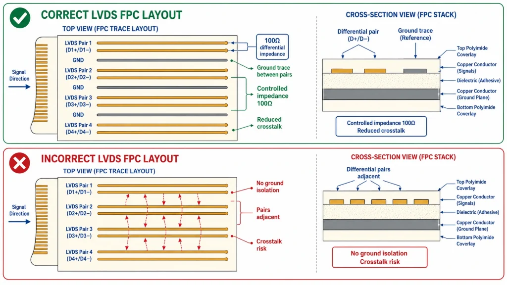
Flat-panel LVDS uses differential data and clock pairs whose rate depends on pixel clock, mapping, color depth, and link configuration. Connector and FPC design must preserve the differential target, pair symmetry, return path, and pair-to-pair isolation required by the transmitter and receiver reference designs.
Ground conductors placed between or adjacent to differential groups can improve return-path continuity and reduce crosstalk, but no fixed percentage improvement applies. The correct pin allocation follows the complete connector/FPC field solution, reference plane geometry, and crosstalk analysis.
MIPI DSI Interface Connectors — Maximum Signal Integrity Demands
No universal layer rule — Do not write “MIPI requires two layers” as a standard requirement. Require a validated controlled-reference structure and channel performance; the fabrication stack-up that achieves it is a design decision.
Related Kadi Display reference: Kadi Display’s MIPI D-PHY and PCB layout reference.
MIPI DSI can place multi-gigabit edge energy through a compact connector and flex. Select the connector using high-frequency data—such as insertion loss, return loss, and crosstalk over the relevant spectrum—together with the host, panel, FPC, and PCB breakout.
A controlled-impedance MIPI channel needs a defined reference structure. A two-layer or multilayer FPC is a common practical solution, but the requirement is electrical rather than a universal layer-count rule. Approve the stack-up, trace geometry, copper, dielectric, coverlay, connector launch, and fabrication tolerance through field-solver or supplier data and prototype validation.
Capacitive Touch FPC Connectors — Low Pin Count, Unique Requirements
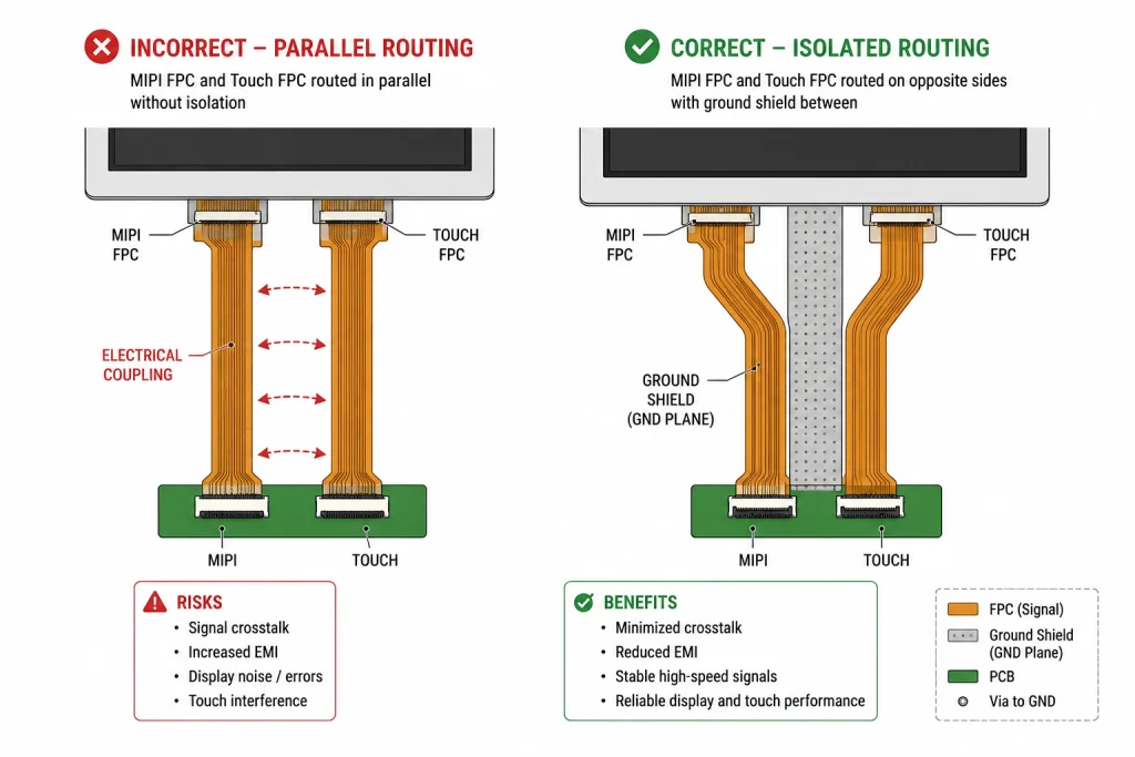
A capacitive-touch controller FPC usually carries I²C or SPI, interrupt, reset, power, and ground. Although the digital bus is relatively slow, the touch sensor measures small capacitance changes and can be sensitive to conducted or radiated noise, grounding, cable movement, and ESD.
Noise control requires a system approach: sensor-stack tuning, ground/reference design, FPC placement, power filtering, controller settings, display timing, backlight behavior, and enclosure bonding. Avoid a universal spacing or star-ground rule without measuring the actual module.
Interface-to-Connector Compatibility Matrix
The following reference matrix consolidates the connector requirements across all four interface types, allowing engineers to make quick comparisons during the schematic planning phase.
Verification Practices — What to Check Before Production Commitment
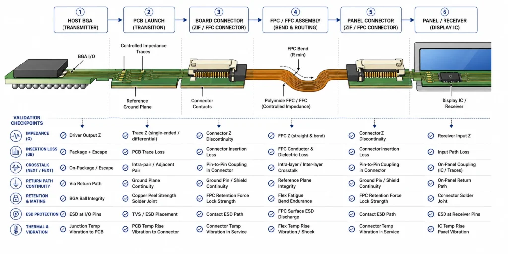
Channel evidence — For a high-speed link, qualify the complete path: transmitter package and PCB launch, board trace, connector, FPC, second connector or panel tail, receiver launch, and return path.
Related Kadi Display reference: Kadi Display’s connector failure-mode diagnostic guide.
Signal integrity failures at FPC connectors often appear only in production — not during bench prototyping — because prototype builds use hand-placed cables with controlled routing, while production builds route FPCs through tight mechanical constraints.
DC continuity and contact resistance confirm basic connection quality but cannot establish high-frequency channel performance. For LVDS and MIPI DSI, use supplier S-parameters, TDR/VNA work where appropriate, receiver eye or protocol error evidence, and production-intent FPC/connector geometry.
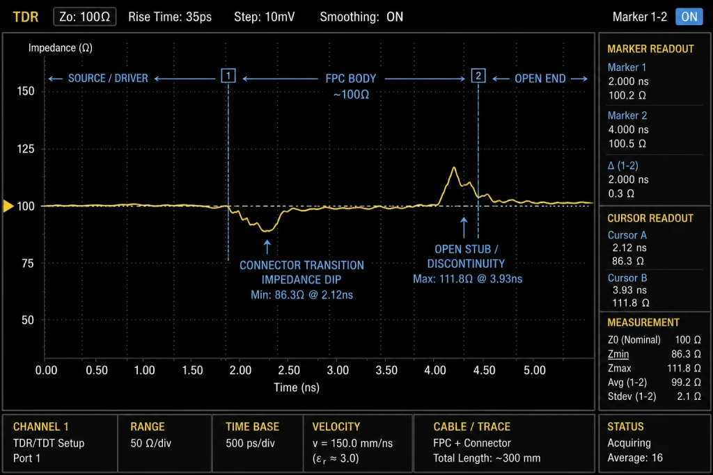
A connector’s DC contact resistance is important for power delivery and basic continuity, but it does not describe insertion loss, return loss, mode conversion, or crosstalk at the signal spectrum. Request the high-frequency characterization needed for the lane rate and inspect the exact PCB footprint used in that characterization.
Production validation should use the final flex length, bend, stack-up, connector alternatives, enclosure pressure, and assembly method. A flat bench cable can pass while a folded production cable fails because the bend changes geometry or pulls the termination partly out of the connector.
For touch, validate with the display and backlight running through worst-case patterns, the DC-DC converters active, chargers and radios transmitting, and the operator/environment conditions expected in the product.
Begin the connector review with the pin field, not the catalog family. Mark every signal by function: high-speed pair, single-ended clock or control, power, return, shield, touch, backlight, and reserved. Then review whether the adjacent contacts and reference structure support the intended current return and isolation. A pinout optimized only for routing convenience can create a difficult high-speed launch.
For RGB, build a timing budget from the transmitter clock-to-data relationship, connector/FPC delay variation, receiver setup and hold, and expected skew. The pixel clock may look modest while the data edges are fast. Long parallel flexes also create simultaneous-switching return current and crosstalk that do not appear in a simple frequency comparison.
For flat-panel LVDS, confirm mapping as well as electrical quality. Different panel conventions can map color bits and control information differently while using connectors that look identical. Record pair polarity, channel/link mapping, color depth, and clock relationship. A clean differential waveform cannot repair an incorrect logical mapping.
For MIPI DSI, treat the connector launch as a geometry transition. Pad width, solder mask, reference-plane voids, ground-via placement, neck-down, and the FPC contact field all influence discontinuity. If a connector vendor supplies S-parameters, verify the fixture, bandwidth, pin assignment, and reference impedance before using them in a channel model.
For touch, separate the controller communication bus from the sensor electrodes. The FPC segment carrying I²C or SPI may be slow, but the sensor tail and electrode network can be sensitive to display noise and mechanical movement. Coordinate the display module supplier’s sensor tuning with the host-board grounding, cover glass, bonding, and enclosure.
Mechanical qualification should include the actuator and cable route. Define how the operator inserts the flex, confirms depth, closes the lock, and supports the exit. Add an insertion mark or fixture where practical. Do not use the connector as a strain-relief clamp, and do not place a sharp fold inside the stiffened termination or at the housing edge.
Alternate components require channel re-evaluation. Two connectors with the same pitch, height, and footprint can differ in contact geometry and high-frequency behavior. Two FPC vendors can build the same drawing with different copper, dielectric, coverlay, adhesive, and thickness tolerances. Approved alternatives should be named parts with test evidence.
Production control closes the loop. Incoming inspection can verify part number, dimensions, contact finish, actuator condition, and FPC stack-up records. Assembly inspection can verify orientation, depth, lock position, and cable support. Functional testing should include patterns or error monitoring that expose intermittent data, not only a static logo.
Evidence Package and Release Control
Before releasing a display fpc connectors design, convert the article’s guidance into a requirements matrix. Give every requirement an owner, source, revision, unit, tolerance, verification method, sample quantity, and acceptance rule. This prevents an informative article from being mistaken for a product specification and makes unanswered questions visible while changes are still inexpensive.
Separate documented limits from planning assumptions. A datasheet value, vendor application note, calculated estimate, measured prototype result, and internal design target do not have the same authority. Label each one. When a value is only representative, record the condition that would make it change and identify the exact document or test that must replace it before production release.
Use production-intent samples for the final decision. Evaluation boards, hand-selected cables, open-bench wiring, laboratory power supplies, and debug firmware can hide tolerance and assembly problems. Repeat the relevant checks with approved component alternatives, final connector and flex routing, enclosure constraints, released clock and power settings, and the intended manufacturing process.
Define failure evidence before testing. Decide which measurements, logs, images, waveforms, error counters, and sample identifiers will be collected when a unit fails. If the team records only pass/fail, intermittent or environment-dependent behavior becomes difficult to reproduce. Good failure evidence should distinguish component, interconnect, firmware, assembly, and system-level causes without immediately blaming the most visible part.
Control changes after approval. A supplier substitution, firmware update, timing adjustment, coating change, connector revision, PCB stack-up change, or new assembly site can invalidate earlier evidence. The change process should state which reviews and tests repeat, who approves deviations, how old and new lots remain traceable, and what field or incoming data will be monitored after release.
For publication, keep MIPI FPC connector terminology consistent with the engineering record. Do not turn a conditional finding into a universal rule to make the prose sound decisive. Search engines and answer systems reward clear direct answers, but technical credibility depends on preserving scope, units, test conditions, and uncertainty. A qualified answer is more useful than a confident number that belongs to another component.
Complete the review with an independent reader. Ask someone who did not write the article or perform the first test to reproduce one calculation, locate each cited requirement, and challenge the main conclusion. Close any gap between the published guidance and the controlled engineering documents. This simple review often catches unit mistakes, stale revisions, hidden assumptions, and claims that cannot be verified from the evidence provided.
Archive the released package in a location shared by engineering, quality, procurement, and support. Include the article revision, approved drawings, links, calculations, test records, known limitations, and decision owner. That package gives later teams enough context to investigate a field issue or approve a controlled change without rebuilding the original reasoning.
Plan the transition from prototype to pilot build. Define which checks remain engineering measurements and which become manufacturing controls, incoming inspection, or end-of-line functional tests. Set escalation rules for intermittent results and retain representative failed samples. A design that works only when a specialist adjusts it by hand is not ready for production; the approved procedure must make correct assembly, configuration, diagnosis, and recovery repeatable for the people who will actually build and service the product.
FAQ: FPC Connector Design by Interface
Is RGB exempt from signal-integrity review?
No. It is often more forgiving than serialized links, but fast edges, cable length, ground distribution, and simultaneous switching still determine timing and noise margin.
Does every MIPI DSI FPC need exactly two layers?
No universal layer count applies. The channel needs a controlled reference structure and verified performance; two or more layers are common ways to achieve it.
Can contact resistance qualify a connector for MIPI DSI?
No. Contact resistance is a DC metric. High-speed qualification also needs insertion loss, return loss, crosstalk, launch geometry, and system validation.
Should every LVDS pair have a ground pin between it and the next pair?
Ground allocation is a useful design tool but must be evaluated with the full pin field, reference planes, connector geometry, and crosstalk budget.
How should touch and display FPCs be separated?
Use module-specific routing and measured noise performance. Physical separation, reference conductors, filtering, controller tuning, and scan timing may all contribute.
Engineering source notes
Related Kadi Display reference: display interface selection for MIPI, RGB, and LVDS.
Related Kadi Display reference: MIPI D-PHY and PCB layout guidance.
Related Kadi Display reference: LCD connector failure modes and diagnostics.
Primary technical references: MIPI D-PHY overview; ST DSI host and interconnect application note; Raspberry Pi display connector documentation.
Product Reference & Engineering Support — For industrial TFT LCD modules, interface documentation, application review, sample validation, and OEM/ODM support, contact Sales@sz-kadi.com or review the Kadi Display product range.
Product range: industrial TFT LCD modules and custom display solutions.
Representative interconnect guidance only. Pin count, impedance, skew, loss, crosstalk, current, ESD, mating durability, and environmental limits depend on the exact host, panel, connector, FPC stack-up, footprint, and test method.
السابق
MIPI DSI and Capacitive Touch: Why the Interfaces Are Separate
التالي
LCD Ribbon Cable Connector Guide: How to Specify ZIF, FFC/FPC, Pitch, and Contact Direction
اترك تعليق

آخر مدونة وأخبار
- MIPI DSI Display Works at Room Temperature but Fails After Warm-Up: A Troubleshooting Workflow
- LCD Prototype Passed but Pilot Units Fail: A Display Integration Isolation Workflow
- VESA vs JEIDA LVDS Mapping: Evidence-Based Color Diagnosis and Release
- eDP LCD Panel Integration: Power, AUX, Link Training, Video and Backlight
- How to Choose an LCD Controller Board: Architecture, EDID, Timing and Latency
مدونة ذات صلة وأخبار
-
 TN مقابل IPS2024-7-9
 -
TN مقابل IPS2024-7-9