
الصفحة الرئيسية
-
مدونة & أخبار
-
VESA vs JEIDA LVDS Mapping: Evidence-Based Color Diagnosis and Release
VESA vs JEIDA LVDS Mapping: Evidence-Based Color Diagnosis and Release
2026-09-20
10:27
VESA vs JEIDA LVDS Mapping: Evidence-Based Color Diagnosis and Release
SEPARATE GATES TE GATES Mapping · color depth · channel count · link integrity
Define Mapping Without Relying on the Labels Alone
NOTATION & ASSUMPTIONS UMPTIONS Treat “VESA” and “JEIDA” as clues, not complete compatibility statements. The release evidence is the exact transmitter or bridge bit assignment, color depth, channel count, cable pinout and panel receiver mapping for the named revisions. Vendor terminology and register names can differ. Do not infer the mapping from connector shape, resolution or an unlabeled “LVDS output.”
First Separate Logical Mapping From the Physical Interface
Flat-panel LVDS, also called OLDI in some component documentation, serializes parallel pixel information across differential channels plus a clock. Several independent choices determine whether the receiver reconstructs the intended pixels.
A connector can be pinned correctly while the logical mapping is wrong. The opposite is also possible: both endpoints may be configured for the same mapping, yet swapped channels or an incorrect cable pinout corrupt the image. Diagnose each layer separately.
KadiDisplay’s industrial display interface guide provides broader LVDS system context. For controller-board paths, the custom TFT-to-controller and ProAV guide helps distinguish source modes, scaling, bridge/controller output and the raw panel interface.
Use Symptoms to Classify, Not to Prove
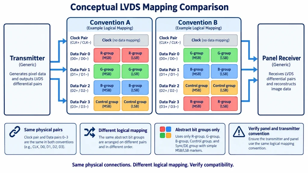
Stable wrong colors, bit-depth artifacts, split images and intermittent link errors belong to different diagnostic branches even when all are first described as an LVDS problem.
What a VESA-versus-JEIDA Mismatch Changes
The two commonly named mappings place significant and less-significant color bits differently in the serialized channel positions. When one endpoint transmits according to one table and the other decodes according to the other, color significance is reassigned. The clock and synchronization can still be good enough to show a stable geometric image, which makes the fault look like a panel-color or software problem.
Do not use memory to infer exactly which shade becomes which color. Generate controlled pixel values and compare the measured or photographed output with the expected bit-level transformation from the two exact mapping tables. Device-specific dithering, color processing, panel gamma and camera exposure can otherwise confuse the pattern.
Do Not Confuse Mapping With 18/24-Bit or Dithering
Mapping and effective pixel depth are related configuration fields but not synonyms. A panel may accept a documented 18-bit or 24-bit style stream, a transmitter may offer dithering or truncation, and a controller may expose both depth and mapping selections. The permitted combinations are device-specific.
If a 24-bit source is reduced to an 18-bit panel path, the missing lower-order information may appear as banding unless appropriate dithering is used. That behavior differs from a mapping mismatch, which reassigns bit significance according to the wrong table. Likewise, enabling a mapping option cannot repair an unsupported depth or packing mode.
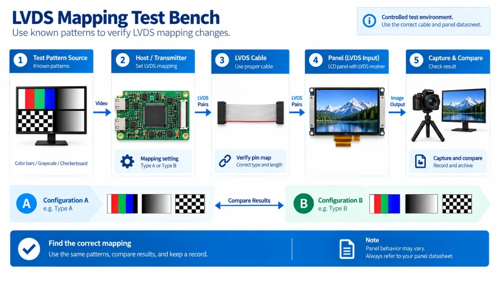
Use a smooth grayscale gradient, stepped near-black and near-white patches, saturated primaries, secondary colors, and values that independently toggle significant bits. Record whether the source pattern is generated before or after GPU color management, scaling, gamma, range conversion or dithering. A screenshot alone may show what software intended, not what the physical panel received.
Treat Single- and Dual-Link LVDS as a Separate Gate
Higher-throughput panels may use two LVDS links/ports, often allocating pixels between them according to the panel specification. The exact assignment—such as odd/even pixels or another documented convention—must match the transmitter and cable. A dual-link fault can create half-screen, column-pair, repeated, interleaved or geometry-related symptoms that are not repaired by switching VESA/JEIDA mapping.
Build a Controlled Mapping Record
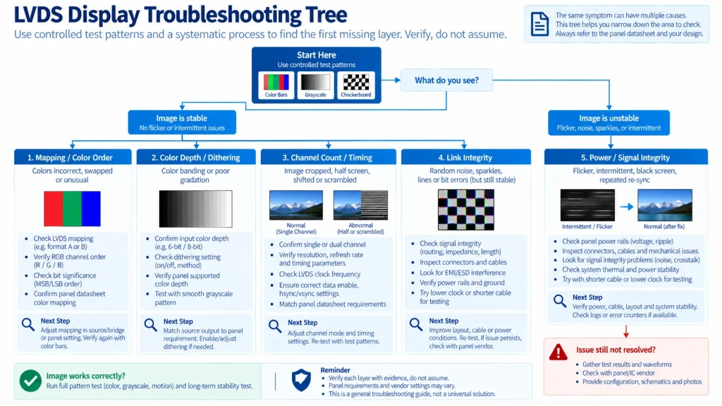
The transmitter, cable and panel mapping must be aligned from controlled documents and actual configuration state before testing.
Build a Controlled Mapping Record Before Testing
Collect the exact panel specification and revision, transmitter/bridge/controller datasheet, board schematic, cable drawing, connector drawing, configuration register or firmware source, controller-board model/revision, and known software state. Extract the mapping tables side by side; do not rely only on a “VESA/JEIDA” dropdown label.
Some panels provide a format-select pin such as an LVDS-format selector, while others require one fixed format. Some bridges or controller boards set the mapping through straps, registers, firmware or an EEPROM panel profile. Verify logic levels, sampling time, pull-up/down ownership, and whether the setting is actually applied after reset. A KadiDisplay module specification can show a product-specific LVFMT selection, but that example must not be transferred to another module without its documentation.
Create a record like this before modifying hardware:
إن FPC and connector design guide is useful when building the physical crosswalk. Verify contact side and numbering views: many cable errors begin when two drawings are both correct but viewed from opposite sides.
Test Mapping Before Touching Signal Integrity
Known digital patterns and one-variable changes can test mapping without random hardware modifications or unsafe probing.
Use a Safe, Evidence-First Test Sequence
Changing multiple straps, cable pins, timing values and software color controls at once destroys diagnostic value and can create electrical risk. Use a known safe power state and change only documented, reversible configuration variables.
- Confirm identity and limits. Match the panel, transmitter/board, cable and documents. Verify power, connector, link topology and timing before testing a format option.
- Freeze software image processing. Use native resolution, a known RGB path where applicable, no adaptive color enhancement, and a deterministic pattern generator. Record range, depth, gamma/LUT and dithering state.
- Prove image geometry and stability. Confirm active area, orientation, line/frame stability and absence of link noise. If unstable, fix timing, SI, power or topology first.
- Run diagnostic patterns. Display saturated R/G/B, white/black, secondary colors, grayscale steps/ramps, fine text and bit-sensitive patches. Photograph under controlled exposure only as supporting evidence.
- Compare exact mapping states. If both endpoints support a documented selection, set one valid combination at a time, reset as required, and record register/strap/pin state plus results.
- Verify physical channels if mapping does not explain the result. Trace schematic-to-cable-to-panel channel order, polarity support, clock pair, grounds and dual-link allocation.
- Expand to product conditions. Test every required timing/mode, boot/recovery, brightness, voltage and temperature corners, cable/connector process, EMI/EMC risk and production configuration.
Separate Mapping Faults From Flicker and Link Integrity
Pure logical mapping errors are generally repeatable for the same pixel value and configuration. Random sparkles, intermittent lines, temperature- or cable-sensitive corruption, loss of lock, flicker, or brightness pulsing point toward other layers. KadiDisplay’s LVDS display flicker diagnostic guide covers timing, signal integrity, cable/connector, power, EMI and backlight branches.
Color faults can also come from RGB/BGR ordering, YCbCr-to-RGB conversion, limited versus full range, GPU LUT/gamma, panel inversion defects, source scaling, controller firmware, damaged channels, or an incorrect panel profile. A mapping diagnosis is strongest when the exact source and sink tables predict the observed transformation and one controlled setting change restores all diagnostic patterns without concealing another failure.
أسئلة متكررة
These answers separate a logical mapping diagnosis from changes that could create an electrical or configuration risk.
Can the wrong VESA/JEIDA setting damage an LCD panel?
A logical mapping mismatch normally concerns decoded pixel/control content, but changing undocumented pins, voltages, power sequence, connector wiring or live cables can damage hardware. Modify only documented controls under a safe procedure.
Why is the image stable if the mapping is wrong?
Clock, timing and channel integrity may be sufficient to reconstruct frames while the receiver assigns serialized color bits the wrong significance. Stable geometry therefore does not prove correct color mapping.
Can an HDMI controller board fix a VESA/JEIDA mismatch?
Only if its panel-output hardware and firmware support the exact required LVDS mapping, depth, topology, timing and panel profile. The HDMI input label does not establish raw-panel compatibility.
Correct One Owned Layer and Freeze It
The fix belongs in one owned layer and must be released with the exact panel, board, firmware/register state, cable and regression evidence.
Choose the Correction at the Owned Layer
Correct the mismatch in the controlled transmitter/bridge/controller configuration when the hardware explicitly supports the required panel mapping. If a panel exposes a documented format-select pin, implement it according to its electrical and reset requirements. If neither endpoint can produce the same mapping, choose a compatible controller/bridge, a different panel, or a formally engineered hardware/logic solution.
Do not “correct” mapping through application color matrices, LUTs, swapped artwork, or image-specific software unless the problem truly belongs to color processing. Such workarounds may fail for video overlays, boot logos, BIOS screens, other operating systems, test patterns, or future firmware. Do not repin differential channels to compensate for logical bit mapping unless exact hardware documentation supports that physical change; bit significance is not generally repaired by intuitive pair swapping.
Release a Mapping Configuration, Not a Tribal Fix
The production record should identify panel and controller revisions, mapping table/reference, select-pin or register state, firmware/profile hash or version, pixel depth/dithering, link topology, cable/board revisions, timing, approved test patterns and expected results. Add receiving identity controls and end-of-line patterns capable of detecting the likely failure. Preserve photographs only with the generating values, camera/setup limits and pass criteria.
Validate cold boot, reboot, sleep/resume, firmware update, failsafe/recovery, every input mode, every approved panel source/revision, brightness states, temperature/voltage corners and pilot production. If an alternate panel uses a different mapping, make the panel-profile selection deterministic and traceable; do not rely on an operator remembering a service-menu setting.
For automated end-of-line detection, choose patterns that create different, unmistakable results under the known wrong configuration. The test must observe the panel output—through a calibrated camera or another justified method—not merely confirm that the source framebuffer contains the right pixels. Control exposure, white balance, ambient light, panel warm-up, viewing geometry and acceptance regions so optical variation does not masquerade as a mapping fault.
Retain a diagnostic signature for each approved configuration: source pixel values, expected region values or tolerances, controller firmware/profile, panel/revision and cable. Revalidate the signature when color processing, dithering, panel source, camera setup or test software changes. A production pattern that caught one historical mismatch may not detect a different channel, depth or dual-link fault, so pair it with identity checks and broader functional evidence.
RELEASE GATE Place the correction in one owned layer—transmitter/bridge configuration, FPGA logic, host firmware or a released cable design—and remove compensating settings elsewhere. Regress solid colors, ramps, text, motion, all supported timings, boot/resume, temperature and cable variants. Release the exact panel, board, firmware/register state, cable drawing and test record together.
KadiDisplay can review panel mapping and cable/controller integration through the engineering contact page; provide the panel specification, transmitter/bridge part, schematic or pin map, register/firmware state, channel count, color depth, timing and controlled-pattern evidence.
Primary Sources
- Texas Instruments display-interface bridge selection guide
- Linux DRM/KMS helpers documentation
- Microsoft display-device design guidance
ENGINEERING DISCLAIMER This article explains a diagnostic method; it does not reproduce a universal VESA or JEIDA mapping table, define the cable pinout, or prove that a visible color error has one root cause. Match the exact transmitter, firmware or strap state, cable, and panel mapping documents. Use known digital patterns and change one documented variable at a time. Power down and escalate before rewiring pairs, changing voltages or termination, hot-plugging unsupported hardware, or applying undocumented register values; validate the corrected mapping together with timing, channel topology, signal integrity, power, and image processing.
السابق
LCD Prototype Passed but Pilot Units Fail: A Display Integration Isolation Workflow
التالي
eDP LCD Panel Integration: Power, AUX, Link Training, Video and Backlight
اترك تعليق

آخر مدونة وأخبار
- MIPI DSI Display Works at Room Temperature but Fails After Warm-Up: A Troubleshooting Workflow
- LCD Prototype Passed but Pilot Units Fail: A Display Integration Isolation Workflow
- VESA vs JEIDA LVDS Mapping: Evidence-Based Color Diagnosis and Release
- eDP LCD Panel Integration: Power, AUX, Link Training, Video and Backlight
- How to Choose an LCD Controller Board: Architecture, EDID, Timing and Latency
مدونة ذات صلة وأخبار
-
 TN مقابل IPS2024-7-9
 -
TN مقابل IPS2024-7-9