
MIPI DSI Bandwidth Guide: Lanes, Pixel Clock, and Data Rate per Lane
2026-08-10
21:26
MIPI DSI Bandwidth Guide: Lanes, Pixel Clock, and Data Rate per Lane
A practical workflow for checking pixel timing, transported data rate, lane count, and implementation margin
MIPI DSI compatibility cannot be decided from active resolution alone. Use the panel timing set, transported pixel format, active lane count, operating mode, and the clock ranges supported by both endpoints. The final setting still has to be verified on production-intent hardware.
The Bandwidth Question That Determines Interface Viability
Direct answer — Calculate the complete-timing pixel clock, convert it to a video-mode planning rate using the transported pixel format, and divide by the active data lanes. Then apply the host-specific packet and clock rules. The selected operating point must fall inside the overlapping host and panel lane-rate ranges.
Related Kadi Display reference: Kadi Display’s MIPI platform support guide.
Complete this check before schematic release. Besides the arithmetic, host and panel must agree on DSI mode, PHY generation, active lane count, timing, packet and pixel format, and software configuration. Use the exact Htotal and Vtotal, transported bits per pixel, and supported lane count; a three-lane link is valid only when both endpoints and the board support it.
MIPI DSI Lane Architecture — Clock Lane Plus 1 to 4 Data Lanes
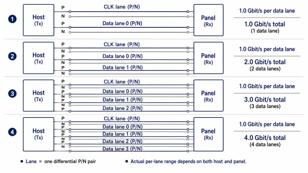
Lane-count note — One D-PHY lane is one differential pair. A conventional link can use one to four data lanes. Two- and four-lane panels are common, but a three-lane link is valid when the host, panel, pinout, and software all support it.
In forwarded-clock mode, the physical link contains one clock pair and one to four data pairs. Adding lanes increases aggregate capacity; it does not raise the maximum rate of each lane. That limit comes from the D-PHY generation and the operating ranges implemented by the host and panel. Embedded-clock features in newer D-PHY revisions require separate treatment.
The D-PHY Clock — How Lane Rate Relates to Clock Frequency
Name the clock — Do not write “DSI clock” without defining pixel clock, HS bit clock, byte clock, escape clock, or PLL reference. Driver APIs and datasheets may use different terms.
For a conventional forwarded-clock D-PHY link in high-speed mode, one data bit is transferred on each edge of the clock lane. The per-lane HS bit rate is therefore twice the forwarded HS clock-lane frequency. This relationship does not apply to byte clock, escape clock, PLL reference clock, or embedded-clock mode.
Per-lane HS bit rate (bit/s) = forwarded HS clock-lane frequency (Hz) × 2
Example: a 500 MHz forwarded HS clock corresponds to 1.0 Gbit/s per data lane. The corresponding HS byte clock is 125 MHz because byte clock equals lane bit rate divided by eight. Some technical reference manuals use “DSI clock” for a PLL or byte-clock value, so confirm the field definition and units before programming it.
Resolution, Color Depth, and Refresh Rate — Calculating Required Bandwidth
Related Kadi Display reference: Kadi Display’s interface selection guide.
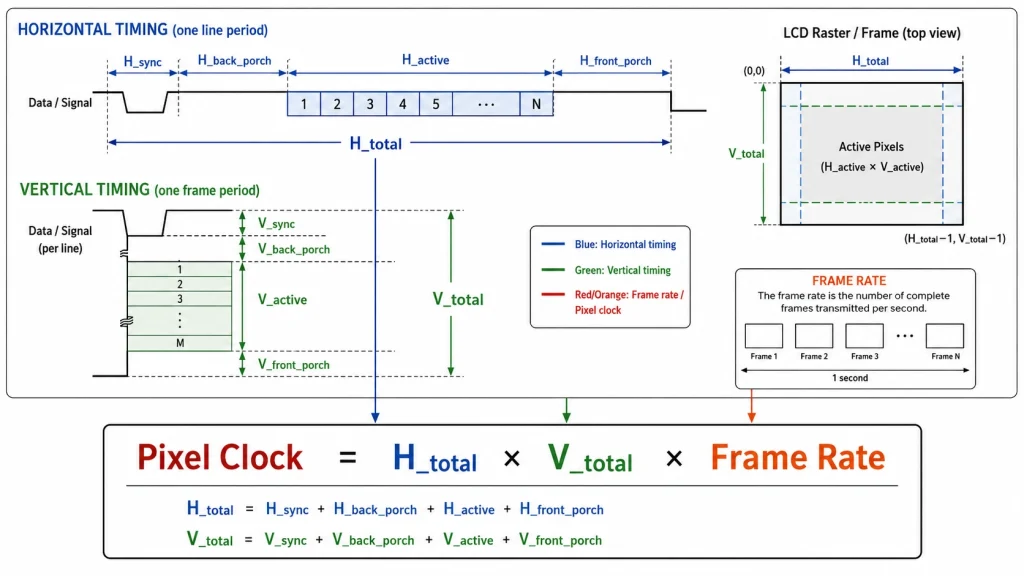
Start from the panel timing table. Htotal and Vtotal include the active area, front porch, back porch, and sync width. Their product with frame rate gives the pixel clock that the source display controller must generate.
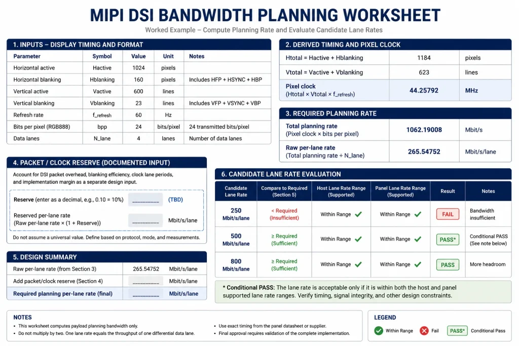
For first-pass video-mode planning: required rate per lane = pixel clock × transported bits per pixel ÷ active data lanes. This is a link-planning value, not the literal active-pixel payload. Active image payload is Hactive × Vactive × frame rate × transported bpp; DSI packet scheduling and blanking behavior depend on the selected video mode and host implementation.
Where:
H_total = Active Width + HBP + HFP + HSW
V_total = Active Height + VBP + VFP + VSW
Transported BPP = 24 for RGB888; 16 for RGB565; 18 for packed RGB666; and 24 for loosely packed RGB666 because it occupies three bytes per pixel. For compressed transport, use the coded bpp and overhead stated by the controller documentation.
FPS = Target refresh rate in frames per second
Worked Example 1 — 720×1280, RGB888, 60 fps, 2 data lanes:
H_total = 720 + 40 + 40 + 10 = 810
V_total = 1280 + 20 + 20 + 4 = 1324
Planning rate per lane = (810 × 1324 × 24 × 60) ÷ 2 = 772.1568 Mbit/s/lane
Forwarded HS clock-lane frequency = 772.1568 ÷ 2 = 386.0784 MHz
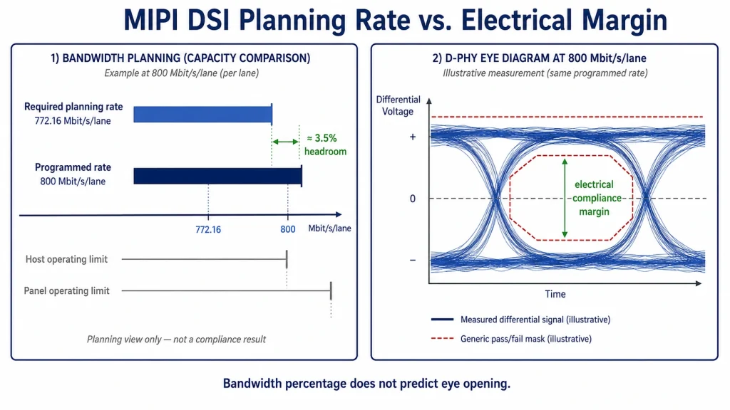
Conclusion: an 800 Mbit/s/lane setting provides only about 3.5% scheduling headroom over this planning value. Treat the operating point as marginal until packet mode, achieved PLL rate, panel receiver range, and stability over production corners are confirmed.
Worked Example 2 — 1080×1920, RGB888, 60 fps, 4 data lanes:
H_total = 1080 + 60 + 60 + 20 = 1220
V_total = 1920 + 30 + 30 + 8 = 1988
Planning rate per lane = (1220 × 1988 × 24 × 60) ÷ 4 = 873.1296 Mbit/s/lane
Forwarded HS clock-lane frequency = 873.1296 ÷ 2 = 436.5648 MHz
Conclusion: a 900 Mbit/s/lane setting leaves about 3.1% scheduling headroom. It may be usable, but the host clock steps, panel range, packet schedule, and measured channel margin still decide whether the configuration can be released.
Common Industrial Panel Resolutions — Pre-Calculated Bandwidth Requirements
The table below uses illustrative timing totals, RGB888, and 60 Hz. It is useful for checking order of magnitude, not for approving a product. Recalculate with the exact panel timing. For one or three data lanes, divide the total rate by one or three.
These are planning rates before host-specific packet rules and clock rounding. Panels with the same active resolution can use different totals, refresh rates, pixel formats, compression settings, or video modes, so their required operating points may differ.
Video Mode Timing — Where the ‘Hidden’ Bandwidth Goes
In video mode, line time is fixed by the programmed pixel timing. Non-burst modes represent sync and blanking with short packets, blanking packets, or null packets according to the host implementation. Burst mode transmits active pixels faster within the line period and may leave idle time, but the host still has to construct a legal line within the available byte-clock cycles.
Do not assume that burst mode removes protocol overhead or guarantees low-power gaps. Confirm the panel-supported mode, clock-lane behavior, LP/HS transitions, packet limits, and the lane-rate method used by the BSP or controller driver.
Margin Engineering — How Much Extra Bandwidth to Provision
Do not program the link exactly at the spreadsheet minimum. Packet bytes, HS entry and exit timing, PLL steps, clock tolerance, and implementation details can consume the remaining schedule. At the same time, a higher bit rate generally makes the electrical channel harder to pass.
Choose the operating rate from the exact planning calculation, the host’s packet and clock method, the panel-supported HS range, and measured channel performance. If platform documentation provides no margin rule, a 10–20% reserve can be used for early screening, but it is not a release criterion or a universal MIPI requirement.
Quick-Reference Design Rules
Release rule — Store the calculation sheet with the exact panel timing revision, pixel format, lane count, host clock settings, DSI mode, overhead assumption, and measured validation result.
Related Kadi Display reference: Kadi Display’s D-PHY and PCB layout guide.
Use the following points as a schematic-review checklist. During bring-up, replace every planning assumption with the exact device documentation or a measured result.
Bandwidth values should be expressed consistently in bit/s, not mixed with byte/s or ambiguous “MHz.” State whether the number is total link payload, per-lane raw bit rate, byte clock, or pixel clock. Unit errors are among the fastest ways to approve an impossible configuration.
More data lanes reduce the rate required on each lane, but they consume pins and routing and may not be supported by the selected panel configuration. One-, two-, three-, and four-lane links are possible; use the configuration supported by both endpoints and actually routed on the board.
After bring-up, monitor host DSI error counters and repeat with worst-case cable, connector alternatives, supply corners, temperature, and graphics patterns. An image that looks correct for five minutes is not a bandwidth qualification.
Build the calculation from the panel timing table, not from a resolution database. Confirm whether the datasheet lists minimum, typical, and maximum pixel clock or only one recommended timing. If several timing sets are allowed, calculate each candidate and preserve the one actually programmed by firmware.
Use transported bits per pixel, not the panel’s advertised color count. RGB565 uses 16 bits/pixel, packed RGB666 uses 18, loosely packed RGB666 occupies 24 transmitted bits/pixel, and RGB888 uses 24. Compressed modes need their coded bpp and packet overhead documented separately.
Command mode needs a different workload view. A command-mode panel can update regions instead of streaming every pixel continuously, but the application must account for changed-area size, update frequency, command overhead, panel memory, tearing synchronization, and worst-case full-screen refresh. Do not reuse a video-mode formula without labeling its assumptions.
Video-mode packetization can make two hosts calculate different required lane rates for the same visible timing. Burst, non-burst sync-pulse, and non-burst sync-event modes treat blanking and null packets differently. Use the host vendor’s calculation method and check that the panel supports the selected mode.
Clock rounding can erase apparent margin. A PLL may generate only discrete lane rates, and the driver may apply dividers or byte-clock rules that move the programmed value away from a spreadsheet result. Record the requested value, achieved value, tolerance, and allowed panel range.
The link must fit at both ends. Some hosts specify a maximum lane rate but also a minimum or operating window; panels can have their own HS range. A calculation below the maximum still fails if the selected setting is below the receiver’s valid range or outside the controller’s PLL constraints.
Signal-integrity margin is not the same as extra bandwidth. Raising lane rate may create more timing room for payload while reducing electrical eye margin through higher loss and jitter sensitivity. Choose the lowest supported rate that satisfies transport needs with validated clocking and channel performance.
Maintain one source of truth for the worksheet. Include units in every cell and make conversion explicit: pixels/s, bits/pixel, bits/s total, bits/s/lane, bytes/s, MHz clock. Have a second engineer reproduce one worked example before releasing the result.
Release Checklist and Test Record
Keep one worksheet tied to the exact panel datasheet revision and firmware configuration. Record horizontal and vertical timing, transported pixel format, DSI mode, active lanes, requested and achieved lane rate, byte clock, and the operating ranges of both endpoints.
Separate sourced limits from assumptions. Mark whether each value came from a panel datasheet, host reference manual, application note, driver calculation, or measurement. If a value is provisional, identify who will replace it and what evidence is required.
Validate with the production-intent PCB, FPC, connector, power settings, and enclosure routing at voltage and temperature corners. Save the DSI error status, achieved clocks, test pattern, sample ID, and exact failure condition. A stable image on one bench unit is not enough.
Repeat the review after a change to the panel or controller revision, FPC, connector, PCB stack-up, PHY clocking, firmware timing, or DSI mode. These changes can invalidate an earlier result even when active resolution is unchanged.
FAQ: MIPI DSI Bandwidth Calculations
Should blanking be included?
For video-mode planning, calculate pixel clock from complete horizontal and vertical timing. Blanking is not active image payload, but it defines the available line and frame time. Follow the selected host’s method for representing blanking and packet overhead.
Is lane data rate always twice the clock?
For a conventional forwarded HS clock-lane frequency, yes: lane bit rate is twice the clock frequency. HS byte clock is lane bit rate divided by eight. The relationship is different if a register exposes PLL reference, byte clock, escape clock, or an embedded-clock value.
Can active resolution alone estimate bandwidth?
It is useful for a rough lower bound, not for compatibility approval. Complete timing and mode are required.
How much margin is enough?
There is no universal percentage. Include transport overhead, available PLL steps, panel range, channel quality, and measured operating-corner stability.
Does more lane count increase refresh rate automatically?
No. It reduces the required rate per lane for a fixed payload. The panel timing, host, and software still set the actual refresh rate.
What if my host controller cannot generate the exact lane rate from the calculation?
Host DSI PLLs typically generate discrete frequency steps, not continuous values. Choose the next higher available rate that is still within the panel’s supported HS range. If the next higher rate exceeds the panel’s maximum, you must reduce payload—by lowering refresh rate, using compression, or adding a lane.
Engineering source notes
Related Kadi Display reference: MIPI DSI platform support and host selection.
Related Kadi Display reference: MIPI, RGB, and LVDS display interface selection.
Related Kadi Display reference: MIPI D-PHY selection and PCB layout.
Primary technical references:
- MIPI Alliance — MIPI D-PHY overview
- NXP — AN13573: i.MX 8/RT MIPI DSI/CSI-2
- NXP — AN12940: RT1170 LCD Display System based on MIPI DSI
- STMicroelectronics — AN4860: Introduction to DSI Host on STM32
- Texas Instruments — SNLA356: DS90UB941AS-Q1 DSI Bringup Guide
Product Reference & Engineering Support — For industrial TFT LCD modules, interface documentation, application review, sample validation, and OEM/ODM support, contact Sales@sz-kadi.com or review the Kadi Display product range.
Product range: industrial TFT LCD modules and custom display solutions.
Representative engineering guidance only. Timing, transported pixel format, blanking transport, packet overhead, lane count, PHY generation, clock definitions, and supported lane-rate range depend on the exact host and panel implementation. Verify the worksheet against current endpoint documentation and production-intent hardware.
Précédent
ESP32-S3 RGB LCD + LVGL: PSRAM, Buffers, and Tearing Control
Suivant
Industrial LCD Defect Classification: Spots, Lines, Mura, and Light Leakage
Laisser un commentaire

Derniers blogs et nouvelles
- MIPI DSI Display Driver Development for Embedded Linux What Hardware Buyers Need to Confirm
- Why Outdoor LCDs Fog Inside: Condensation, Sealing, Vents, and Heaters
- IP65 vs IP67 Industrial Displays: What the Rating Actually Covers
- How to Specify a Touchscreen for Food-Processing Equipment
- Thermal Management for High Brightness LCDs in Sealed Outdoor Enclosures